|
|
|
|
|
|
|
|
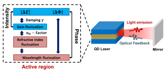
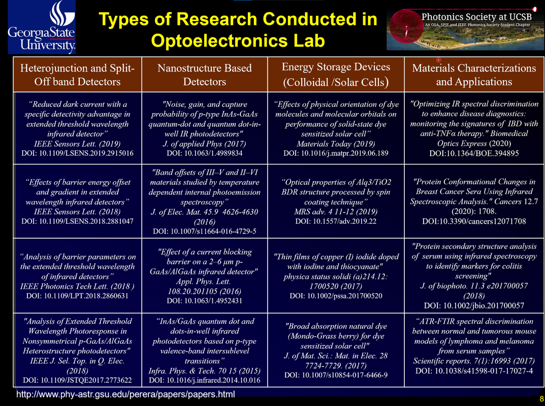
 Friday, August 11th at 1:00pm in Henley Hall Semiconductor nanostructures with low dimensionality like quantum dots are one the best attractive solutions for achieving high performance photonic devices. When one or more spatial dimensions of the nanocrystal approach the de Broglie wavelength, nanoscale size effects create a spatial quantization of carriers. When directly grown on silicon, they even show a four-wave mixing efficiency much superior compared to the conventional quantum well devices. This remarkable result paves the way for achieving high-efficiency frequency comb generation from a photonic chip. Quantum dot lasers are a good candidate for applications in optical routing and optical atomic clock and quantum information processing. This lecture will review the recent findings and prospects on nanostructure based light emitters made with quantum-dot technology and their applications.
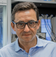
Frédéric Grillot is currently a Full Professor at Télécom Paris (France) and a Research Professor at the University of New-Mexico (USA). His research interests include, but are not limited to, advanced quantum confined devices using III-V compound semiconductors, quantum dots quantum dashes, light-emitters based on intersubband transitions, non-classical light, nonlinear dynamics and optical chaos in semiconductor lasers systems as well as microwave and silicon photonics applications.
Professor Grillot has made outstanding technical contributions in photonics and optical communications. He has intensively contributed to the development of quantum dot devices enabling their utilization as future active devices with superior performance. In particular, his recent achievements on epitaxial quantum dot lasers on silicon are crucial for the development of isolation-free integrated technologies. Among his major achievements, he also reported the first private optical communication using mid-infrared chaotic light, giant pulses emission in quantum cascade devices as well as multigigabits operation in the thermal atmospheric window with unipolar quantum optoelectronics. Overall, his research is a strong input to the advancement of science and to the emerging practical applications in computer and quantum technologies, as well as in more traditional areas such as optical communications. Professor Grillot strongly contributes to promote and support the development of the general optics community. He has served diligently and successfully Optica in particular as an Associate Editor of Optics Express, now as a Deputy Editor since September 2022. As of now, he has published more than 130 journal articles, 3 book chapters, and delivered many invited talks in major international conferences and workshops. Frédéric Grillot is also a Fellow Member of the SPIE as well as a Senior Member of Optica and the IEEE Photonics Society. In 2022, he received the IEEE Photonics Society Distinguished Lecturer Award which honors excellent speakers who have made technical, industrial or entrepreneurial contributions to the field of photonics. 
February 23, 2023 at 9:00 am in Henley Hall 1010 and on Zoom 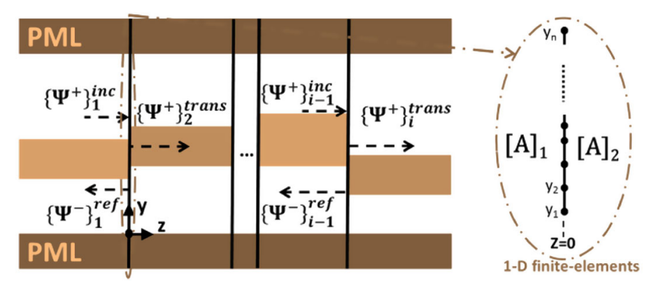 Schematic diagram of optical waveguides with multiple longitudinal discontinuities (i − 1) [12]. The first discontinuity is located at z = 0. {ψ −}i and {ψ +}i are the backward and forward propagating fields, respectively, usually used in BiBPMs. Afaf Said, Khaled S. R. Atia, and S. S. A. Obayya, "On modeling of plasmonic devices: overview," J. Opt. Soc. Am. B 37, A163-A174 (2020) Schematic diagram of optical waveguides with multiple longitudinal discontinuities (i − 1) [12]. The first discontinuity is located at z = 0. {ψ −}i and {ψ +}i are the backward and forward propagating fields, respectively, usually used in BiBPMs. Afaf Said, Khaled S. R. Atia, and S. S. A. Obayya, "On modeling of plasmonic devices: overview," J. Opt. Soc. Am. B 37, A163-A174 (2020) Nanophotonics modelling for 21st century applications is becoming vital. The computational modeling provides a fundamental understanding of the relying physics behind the operation of photonic devices. However, computational modeling is still a challenge as some of the existing modeling techniques fail to capture the correct behavior of nano-photonic devices. In this regard, this talk will introduce an overview of the existing computational modeling tools for analyzing photonic devices, in general, and highlighting their salient features and shortcomings. It is well known that “plasmonics” plays a vital role now in localising the optical field beyond the diffraction limit and hence in integrated optics. Therefore, the talk will focus on plasmonics modeling issues and the failure of the classical electromagnetic solvers to accurately characterize the nano-plasmonic devices. Therefore, new accurate and stable beam propagation method will be introduced for analyzing plasmonics in the classical regime. The rigor of this approach is mainly because of relying on the finite elements method and the twice faster Blocked Schur algorithm which can exactly represent all the wide spectrum of radiation, evanescent, and surface modes produced by the strong discontinuity between metal and its surroundings. Moreover, in merging quantum plasmonic devices, it becomes essential to introduce “Quantum Corrected Model (QCM)” in order to accurately model these devices, and the basics of QCM will be also discussed. Dr. Salah Obayya Biography: Salah S A Obayya joined Zewail City of Science and Technology (ZC) in 2012 where he is now Chair Professor and Founding Director of Center for Photonics and Smart Materials (CPSM). He occupied the positions of the Vice Chairman of ZC and Director-General of Research Institutes at the same institution. Prior to Zewail City, he took up several academic posts at Brunel University UK (tenured Associate Professor, 2002), University of Leeds, UK (tenured Professor, 2006) and University of South Wales, UK (tenured Chair Professor, 2008) where he was the Founding Director of Photonics and Broadband Communications (PBC) Research Center and also he was the Director of Postgraduate Programs at the same institution. In May 2006, he has been naturalized as “British” citizen.
He has established an outstanding international reputation in the area of green nanophotonics with focus on the intelligent computational modeling of modern nano-photonic devices enabling technologies needed to realise low-carbon green society. He has published 271 journal publications, mostly in OSA, IEEE and IET/IEE, authored 3 books (Computational Photonics, Wiley 2010 and Computational Liquid Crystal Photonics, Wiley 2016, Computational of Photonic sensors, 2018) both are adopted references for Graduate Programs in Photonics at international Universities such as MIT, Purdue University, Indian Institute of Technology, National University of Singapore, Mansoura University and Zewail City, and 264 conference papers in international conference in photonics, many of these are invited talks, and keynote lectures, attracted external funding, from both industry and Research Councils, in the region of $ 4M, and supervised to successful completion 35 PhD students, over 70 MSc/MRes/MPhil students and 15 postdoctoral research fellows. He led the team that developed one of the world’s best comprehensive numerical packages for the analysis, design and optimization of nano-photonic devices, and subsystems, where a number of “world-first” numerical approaches have been developed. His five key papers introducing his novel numerical package; have been cited more than 400 times. His publications also have been cited more than 4000 times, with an h-index of 34 and i10-index of 118. His numerical package has been widely adopted by both academic and industrial Photonics communities to analyze, design and optimize the performance of a wide range of nano-photonic devices employed for applications in solar cells, optical telecoms, sensing, optical imaging and encryption and other applications. He has served the International Photonics Society through active contribution to the organization and technical committees of a number of international conferences. Since 2007, he has been an Associate Editor-in-Chief of the IEEE Photonics Technology Letters, and Associate Editor-in-Chief of the Journal of Optical and Quantum Electronics, and served as Guest Editor-in-Chief of J Optical and Quantum Electronics (2010), and founding member of Editorial Board of Materials Theory Journal (Springer) and acted as Reviewer for many international Photonics Journals such as IEEE J Lightwave Technology, IEEE Photonics Journal IEEE J Quantum Electronics, IEEE J Selected Topics in Quantum Electronics, IET Optoelectronics, OSA Optics Express, OSA Optics Letters, and many others. Moreover, he acted as Technical expert and Reviewer for a number of research funding councils and learnt societies such as Engineering and Physical Sciences Research Council (EPSRC), UK, Royal Society, UK, Royal Academy of Engineering, UK, National Academy of Arts and Sciences, Holland, Science and Technology Development Fund, Egypt, National Telecom Regulatory Authority (NTRA), Egypt and others. Quantum wells in Nanowires for Optoelectronic Applications: Materials and Devices - Dr. Lan Fu6/15/2022
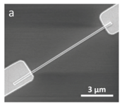
Thursday, June 23rd, 2:00 pm (PDT) -- Burgers from Kyle’s! Hosted in-person in Henley Hall 1010 Abstract – III-V compound semiconductor nanowires (NWs) have drawn much attention as nanoscale building blocks for integrated photonics/optoelectronics due to their nanoscale size, excellent optical properties and effectiveness in strain relaxation enabling the monolithic growth on lattice-mismatched substrates. In particular, NWs grown by selective area epitaxy technique have many advantages such as controllability of their size and position, high uniformity in diameter and length, as well as complementary metal-oxide-semiconductor (CMOS) process compatibility, facilitating their integration with other electronic devices. With suitable wavelength ranging from 1.3 to 1.6 μm and lattice match of constituent materials, InGaAs/InP quantum well (QW) has been being widely used for optical communication devices. However there has been limited understanding on the growth of InGaAs/InP QW in nanowire architecture and their application for optoelectronic devices such as lasers/LEDs and photodetectors. In this work, we present the study of the selective area epitaxy growth of InGaAs/InP multi-QW NW array by metalorganic chemical vapour deposition (MOCVD) technique, and the demonstration of nanowire LEDs/lasers and photodetectors with an investigation of their strong geometry related device properties by both numerical simulation and optoelectronic characterizations. Bio – Lan Fu received her PhD degree from the Australia National University (ANU) in 2001 and is currently a Full Professor at the Research School of Physics, ANU. Prof. Lan Fu was the recipient of the IEEE Photonic Society Graduate Student Fellowship (2000), Australian Research Council (ARC) Postdoctoral Fellowship (2002), ARF/QEII Fellowship (2005) and Future Fellowship (2012). Professor Fu is a senior member of IEEE, IEEE/Photonics and Electron Devices Societies and was the past chair of the Photonics Society, Electron Devices Society and Nanotechnology Council Chapters of the IEEE ACT section. She is the Chair of IEEE Nanotechnology Council Chapters & Regional Activities Committee, Associate Editor of IEEE Photonics Journal, and member of Editorial Board of Opto-Electronic Advances. She also the current member of the Australian Academy of Science National Committee on Materials Science and Engineering, Secretary of the Executive Committee of Australian Materials Research Society (AMRS), and Australian Research Council College of Experts. Professor Lan Fu’s main research interests include design, fabrication and integration of optoelectronic devices (LEDs, lasers, photodetectors and solar cells) based on low-dimensional III-V compound semiconductor structures including quantum wells, self-assembled quantum dots and nanowires grown by metal-organic chemical vapour deposition (MOCVD). Li, Z. Y., Tan, H. H., Jagadish, C., Fu, L., Adv. Mater. Technol. 2018, 3, 1800005. https://doi.org/10.1002/admt.201800005
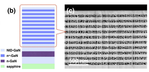
Friday March 4th at 1:00pm PST in Henley Hall 1010 and via Zoom Pizza Provided in-person! Porous semiconducting nitrides are effectively a new class of semiconducting material, with properties distinct from the monolithic nitride layers from which devices from light emitting diodes (LEDs) to high electron mobility transistors are increasingly made. The introduction of porosity provides new opportunities to engineer a range of properties including refractive index, thermal and electrical conductivity, stiffness and piezoelectricity. Quantum structures may be created within porous architectures and novel composites may be created via the infiltration of other materials into porous nitride frameworks. A key example of the application of porous nitrides in photonics is the fabrication of high reflectivity distributed Bragg reflectors (DBRs) from alternating layers of porous and non-porous GaN. These reflectors are fabricated from epitaxial structures consisting of alternating doped and undoped layers, in which only the conductive, doped layers are electrochemically etched. Conventionally, trenches are formed using a dry-etching process, penetrating through the multilayer, and the electrochemical etch then proceeds laterally from the trench sidewalls. The need for these trenches then limits the device designs and manufacturing processes within which the resulting reflectors can be used. We have developed a novel alternative etching process, which removes the requirement for the dry-etched trenches, with etching proceeding vertically from the top surface through channels formed at naturally-occurring defects in the crystal structure of GaN. This etch process leaves an undoped top surface layer almost unaltered and suitable for further epitaxy. This new defect-based etching process provides great flexibility for the creation of a variety of sub-surface porous architectures on top of which a range of devices may be grown. Whilst DBR structures enable improved light extraction from LEDs and the formation of resonant cavities for lasers and single photon sources, recent development also suggest that thick, subs-surface porous layers may enable strain relaxation to help improve the efficiency of red microLEDs for augmented reality displays. Meanwhile, the option of filling pores in nitride layers with other materials provides new opportunities for the integration of nitrides with emerging photonic materials, such as the hybrid-perovskite semiconductors, with perovskites encapsulated in porous nitride layers demonstrating greatly improved robustness against environmental degradation.
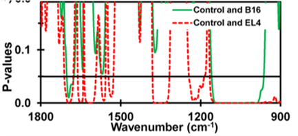
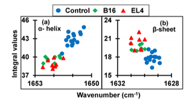
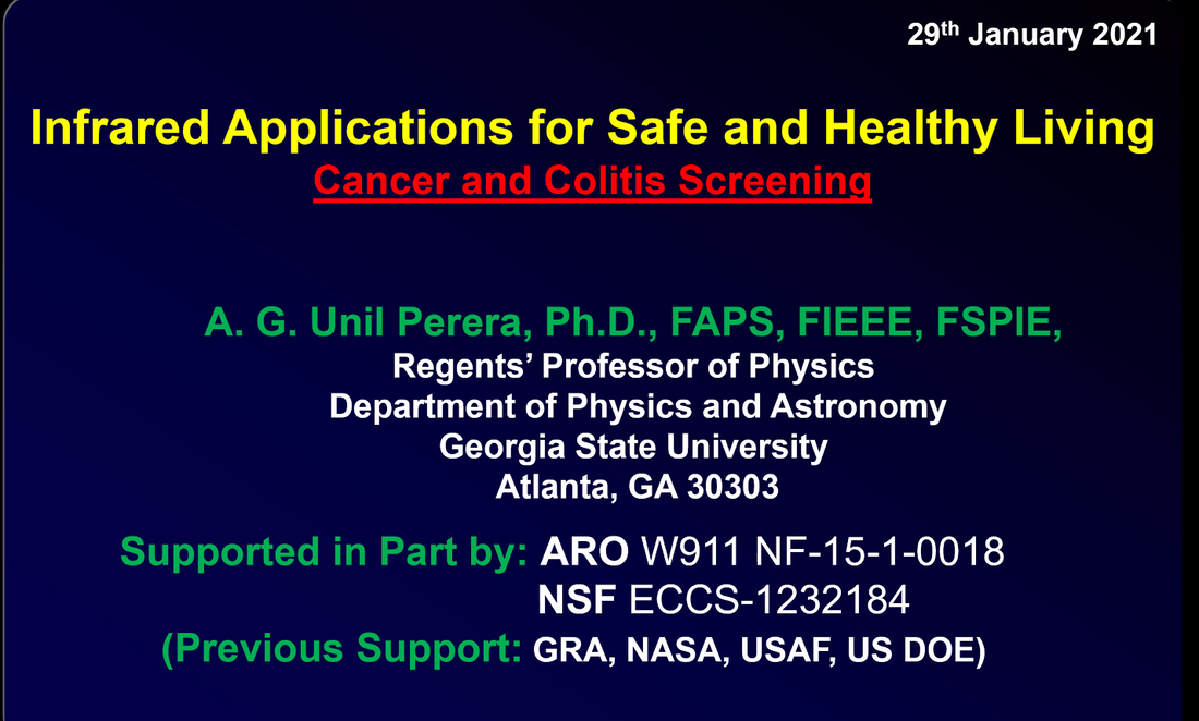
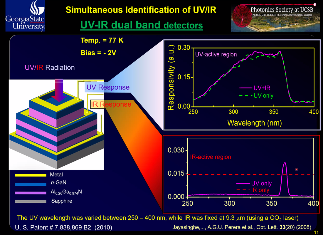
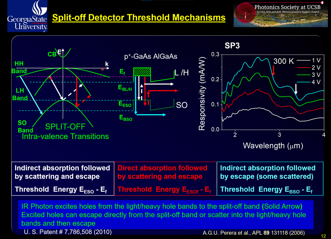
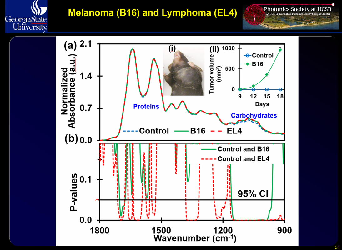
Friday, January 29th, 10 am (PST) Infrared detectors and imaging systems are becoming increasingly important in a diverse range of astronomic, military, and civilian applications. This field has gained significant attention while incorporating various materials and architectures into detector designs with a strong focus on applicability into clinical domains. Dr. Perera will discuss recent detector structures, and his latest work on disease detection. Biomedical applications of infrared include an exploration of an Affordable, Sensitive, Specific, User-friendly, Rapid, Equipment-free, and Deliverable (ASSURED) diagnostic regimen and testing its clinical feasibility for inflammatory bowel diseases (IBDs) and cancer screening. A study using Fourier transform infrared (FTIR) spectroscopy in attenuated total reflectance (ATR) sampling mode analyzed body fluids in order to identify reproducible, stable, and statistically significant differences in spectral signatures of the IR absorbance spectra between the control and disease samples. These results show that serum samples can be used to detect the biochemical changes induced by these diseases.
Tuesday, September 8th, 10 am (PDT) via Zoom Meeting ID: 978 3569 2970 Passcode: 468555 Infectious diseases and water are some of the greatest, most urgent challenges of the 21st century. III-nitride ultraviolet (UV) light sources, including light emitting diodes (LEDs) and lasers, are the only alternative technology to replace conventional power-hungry, hazardous mercury lamps for disinfection and water purification. Recent studies showed that AlGaN-based UV-C LEDs can readily shred genetic material of viruses and bacterial and achieve 99.9% sterilization of SARS-COV-2. In this talk, I will present the recent advances of AlGaN and BN nanostructures and heterostructures and their applications in UV optoelectronics, including the first demonstration of mid and deep UV laser diodes and tunnel junction UV-C LEDs with significantly improved performance. The recent development of far-UV-C LEDs, in the wavelength range of 207-222 nm, will also be presented, which has shown to be faster and far more effective than traditional UV-C light (~265 nm) in preventing the transmission of microbial diseases, while causing virtually no harm to mammalian skin or eye.
Friday, February 7th from 12:00 - 1:00 pm in ESB 2001 The electrical power consumed in data transmission systems is now hampering efforts to further increase speed and capacity at various scales, ranging from data centers to microprocessors. Optical interconnects employing ultra-low-energy directly-modulated lasers will play a key role in reducing the power consumption. Since a laser's operating energy is proportional to the size of its active volume, developing high-performance laser with a small cavity is important. For this purpose, we have developed DFB and photonic crystal (PhC) lasers, in which active regions are buried with an InP layer. Thanks to the reduction of cavity size and the increase in optical confinement factor, we have achieved an extremely small operating energy of 4.4 fJ/bit by employing a wavelength-scale PhC cavity. Cost reduction is also an important issue because a larger number of transmitters are required for short-distance optical links. For this purpose, Si photonics technology is expected to be a potential solution because it can provide large-scale photonic integrated circuits (PICs). Therefore, heterogeneous integration of III-V compound semiconductors and Si has attracted much attention. To fabricate these devices, we have developed wafer-scale fabrication that employs regrowth of III-V compound semiconductors on directly-bonded thin InP templates on an SiO2/Si substrate.  Dr. Matsuo discusses some of the equations related to semiconductor lasers.
Thursday, January 30th, 11 am, Elings 1605 NASA’s trend toward less costly missions has created a need for smaller and more capable instruments for in situ planetary applications, space weather, and Earth Observations. The rise of cubesats has created a new powerful platform that if enabled with powerful sensing technology can be an instrument of discovery. At the same time, large aperture UV/visible/Near Infrared space telescope are being planned for cosmology and astrophysics studies that will need high performance yet affordable detectors to populate their very large focal plane arrays. In nearly all these facets of space exploration, there is a strong need for high signal to noise ultraviolet detection technology. This is due to the fact that the ultraviolet part of the spectrum is rich in spectral information that are key to study exo-solar planets, protoplanets, intergalactic medium, supernovae, electromagnetic counterpart of gravitational wave, star formation, galaxy evolution, and more. Semiconductor detectors offer a rich spectral range, tailorable spectral response, high resolution, and sensitivity; however, these capabilities are not available in a single material or class of material. For example, while silicon imagers have reached high performance levels in format, pixel size, and signal to noise, they are naturally insensitive to ultraviolet light. Using non-equilibrium processes, we can manipulate materials at nanometer scale, form unusual and quantum structures, and alter bandstructures. Through nanoscale surface and interface engineering of 2D doping (superlattice doping and delta doping) high performance silicon-based imagers are produced with record high quantum efficiency in the ultraviolet. Furthermore, the response of silicon imagers can be tailored for out of band rejection through nano-scale interface engineering. In this talk we will discuss the underlying physics of the ultraviolet silicon detectors, their performance, their integration in systems, and their application in cubesats and space flagship missions. We will also discuss the synergy between the requirements for instruments in NASA space applications and medical applications and show how space technologies can and have been used for medical applications. Coffee provided! 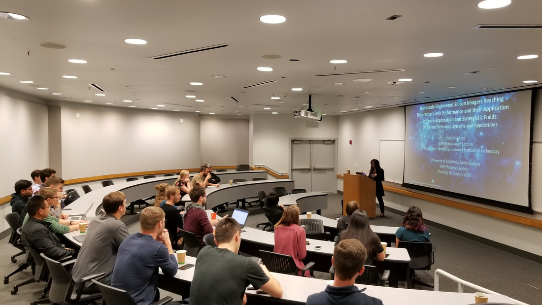 Dr. Nikzad introduces here work at NASA on Si-based UV detectors applications on cubesats. 
Friday April 26th | 12:00 pm | Elings 1605 Two-dimensional Van der Waals materials have emerged as a very attractive class of optoelectronic material due to the unprecedented strength in its interaction with light. In this talk I will discuss approaches to realize quantum photonic devices by integrating these 2D materials with microcavities, and metamaterials. I will first discuss the formation of strongly coupled half-light half-matter quasiparticles (microcavity polaritons) and their optical and electrical control in the 2D transition metal dichacogenide (TMD) systems. Prospects of realizing condensation and few photon nonlinear switches using Rydberg states in TMDs will also be discussed. Following this, I will discuss the broadband enhancement of light-matter interaction in these 2D materials using photonic hypercrystals and chiral metasurfaces. Finally, I will talk about room temperature single photon emission from hexagonal boron nitride and the prospects of developing deterministic quantum emitters using them through strain engineering. The realization of room temperature single photon emitters and few photon nonlinear switches using 2D materials presents an attractive direction for robust next generation quantum photonic technologies. Refreshments Provided! 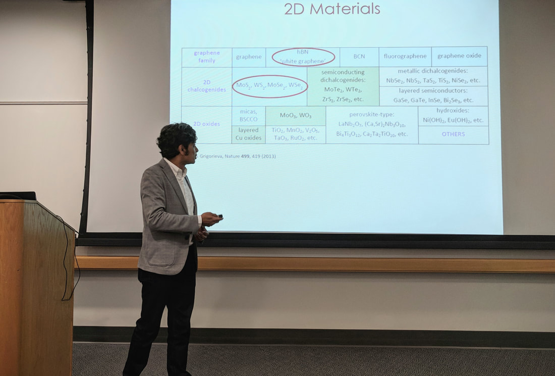 Dr. Menon describes the different categories of 2D materials and identifies Van der Waals materials
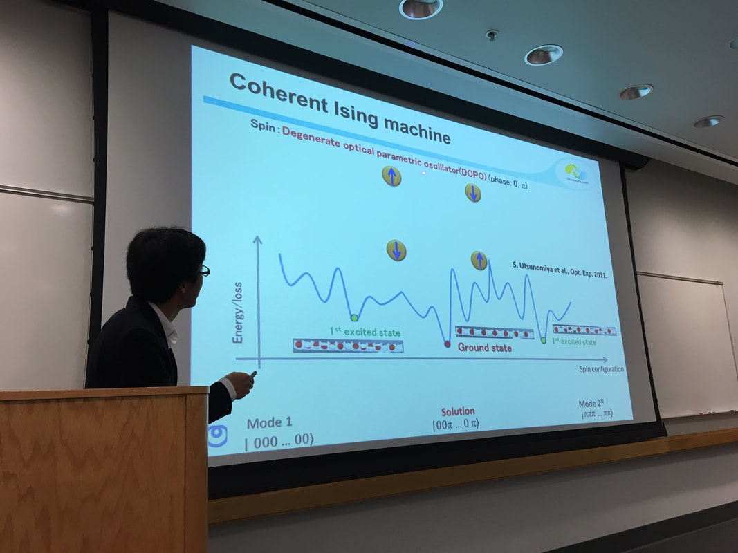
Friday, Jan 18, 12 – 1 pm, Elings 1605 As various systems and networks in our society grow larger and more complex, analysis and optimization of such systems are becoming increasingly important. Such tasks are classified as combinatorial optimization problems, which are generally difficult to solve with current digital computers. It is well known that combinatorial optimization problems can be converted to ground-state-search problems of the Ising model, a theoretical model for the interacting spins. Recently, several approaches to find solutions to the Ising model using artificial spin systems have been studied intensively. A coherent Ising machine (CIM) is one of such systems in which degenerate optical parametric oscillators (DOPO) pulses are used as artificial spins. By using a long-distance (typically 1 km) fiber cavity that contains a phase sensitive amplifier based on a periodically poled lithium niobate waveguide, we can generate thousands of DOPO pulses multiplexed in time domain. Since a DOPO phase only takes either 0 or p at above threshold, we can stably express an Ising spin with a DOPO by allocating phase 0 (p) as spin up (down). The “spin-spin interaction” can be implemented by using a measurement-feedback scheme, with which we can effectively realize mutual injection of lights among thousands of DOPO pulses. The networked DOPOs are most likely to oscillate at a phase configuration that best stabilize the whole network, which gives the solution to the given Ising problem. Based on this scheme, we realized a CIM with all-to-all-coupled 2000 DOPO pulses, by which we could find good solutions to 2000-node combinatorial optimization problems in less than 100 microseconds. In the talk, I will describe the basic principle and the experimental details of the CIM, as well as our effort for finding its applications. Refreshments Provided!  Dr. Ken-Tye Yong Director of the Bio Devices and Signal Analysis (VALENS) School of Electrical and Electronic Engineering Nanyang Technological University (NTU) Tuesday, Nov. 20th, 3 - 4 pm, ESB 2001 Nanomaterials have been applied in healthcare applications such as cancer imaging, lymph node mapping and brain diseases therapy. These nanomaterials can be engineered to serve as a platform for challenges in highly sensitive optical diagnostic tools, biosensors, and guided imaging and therapy. The versatility of nanomaterials may provide the keys to improve diagnostics and therapy of human diseases. In this talk, we will highlight the use of nanomaterials with different sizes, compositions, and shapes for nanomedicine applications. This talk is intended to promote the awareness of past and present developments of nanomaterials in biomedical fields, the potential toxicity of nanomaterials, and the approaches to engineer new types of safe nanomaterials, whereby encouraging researchers to think about exciting and promising biophotonic and nanomedicine applications with nanomaterials in the future. Refreshments Provided!  Friday Nov 9th, 1pm, Elings 1605 The past decade has seen accelerated progress in III-V semiconductor infrared photodetector technology. The advent of the unipolar barrier infrared detector device architecture has in many instances greatly alleviated generation-recombination (G-R) and surface-leakage dark current issues that had been problematic for many III-V photodiodes. Meanwhile advances in a variety type-II superlattices (T2SLs) such as InGaAs/GaAsSb, InAs/GaSb, and InAs/InAsSb, as well as in bulk III-V material such as InGaAsSb and metamorphic InAsSb, have provided continuously adjustable detector cutoff wavelength coverage from the short wavelength infrared (SWIR) to the very long wavelength infrared (VLWIR). The confluence of these developments has led to a new generation of versatile, cost-effective, high-performance infrared detectors and focal plane arrays based on robust III-V semiconductors, providing a viable alternative to HgCdTe (MCT). Refreshments provided!  Prof.Brian Cunningham Department of Electrical and Computer Engineering, Department of Bioengineering University of Illinois at Urbana-Champaign Tuesday, Oct 16th, 11am, ESB 1001  Circulating exosomal miRNA represents a potentially useful class of bloodborne biomarkers for cancer. We present the initial proof-of-concept of an approach in which gold nanoparticle tags are prepared with thermodynamically optimized nucleic acid toehold probes that displace a oligonucleotide and reveal a capture sequence that is used to selectively pull down the target-probe-nanoparticle complex to a photonic crystal (PC) biosensor surface. By matching the surface plasmon resonant wavelength of the nanoparticle tag to the resonant wavelength of the PC nanostructure, the reflected light intensity from the PC is dramatically and locally quenched by the presence of each nanoparticle. The talk described the optical operating principles of Photonic Resonator Absorption Microscopy (PRAM), the thermodynamic design of DNA toehold probes, and our first results demonstrating the detection limits, selectivity, and dynamic range of the assay. Refreshments provided! 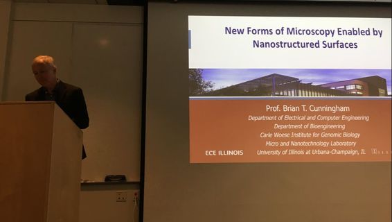 Dr. Cunningham giving his talk about Microscopy Enabled by Nanostructured Surfaces. Friday, Jun. 8th, 4:30 - 5:30 pm, ESB 2001 Communications networks and systems are seeing extreme increases in network traffic which is growing at the tremendous rate of 30% per year. It is estimated that the energy and cost requirements will increase tenfold in coming year. But this progress is not sustainable from an ecological and economic point of view. However, this information explosion can be dealt with, using the integration of very small photonic components on very high density Photonic Integrated Circuits (PICs). The technolgoical advancements in PICs have made them a popular choice for components of next generation networks. Silicon being the evident choice due to its high availability, mature fabrication technology, and low cost has attracted components on a chip. At the same time, the unique, material properties and direct bandgap of group III-V materials have huge potential in applications like laser amplifiers, modulators, and detectors. Due to robustness, flexibility, reliability, and performance of PICs, many commercial solutions are now available for a variety of applications. Refreshments Provided! 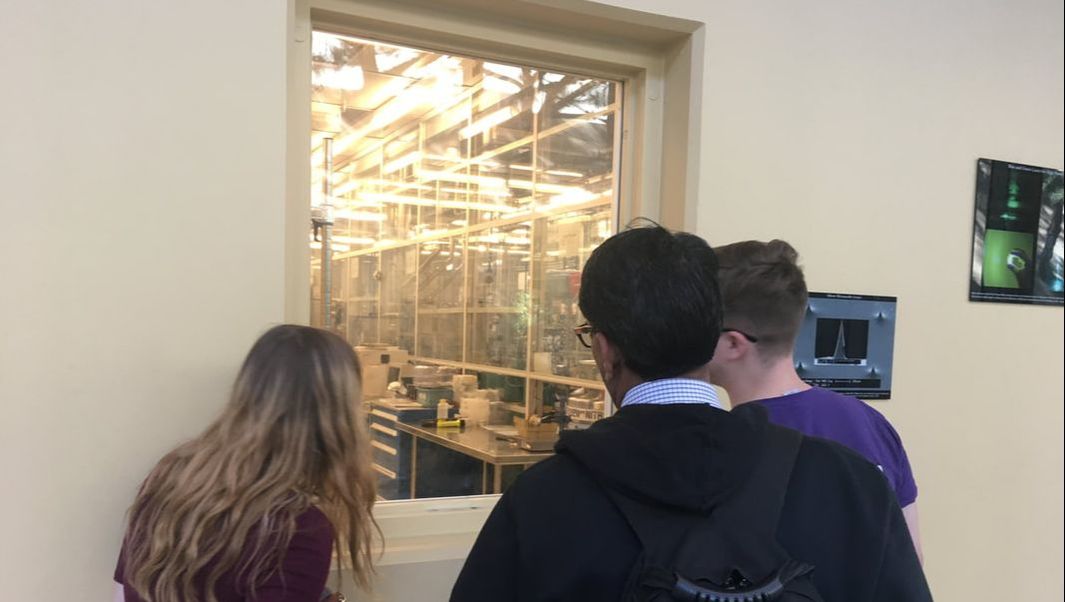 Dr. Singh looking into the UCSB nanofab cleanroom during his visit. |
Mailing ListSupported By
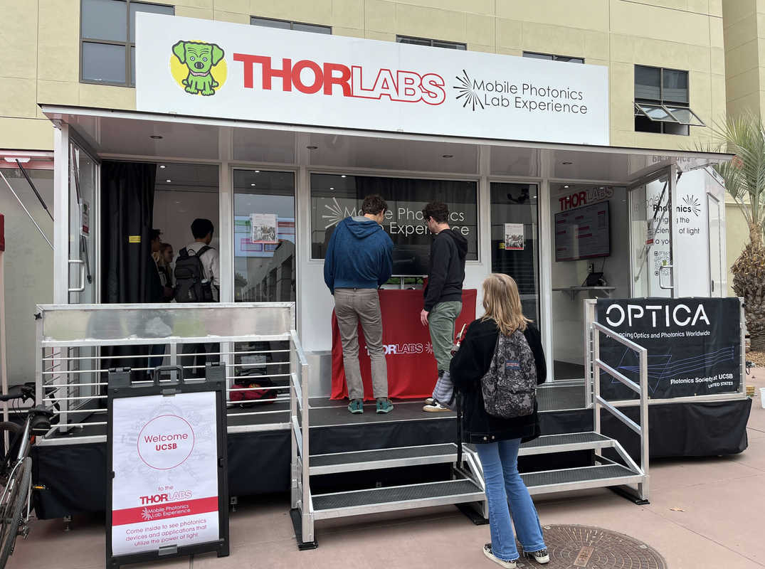
Thorlabs designs and produces a variety of optomechanical and optoelectronic components in 15 facilities around the globe. Thorlabs seeks to listen and serve its customers with over 20,000 products available.

Founded in 2018, Nexus Photonics has developed integrated photonics ready to scale. Smaller, lighter and faster, their platform outperforms industry benchmarks, and operates in an ultra-broadband wavelength range from ultraviolet to infrared to support a wide breadth of practical applications.

Archives
May 2024
Categories
All
|
||||||||||||||||||||||||||