|
Who: J. Stewart Aitchison Department of Electrical and Computer Engineering, University of Toronto When: Monday, March 13, 12:00PM Where: ESB 1001 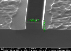 Abstract: The III‐V semiconductor AlGaAs is an ideal nonlinear optical material. It has large second and third order nonlinearities, a low two‐photon absorption coefficient at the half band gap and allows for the easy fabrication of integrated optical devices. In additoon, AlGaAs can be used directly integrate photodiodes, modulators and passive optical elements on the same chip as the nonlinear elements. This talk will highlight the benefits of this nonlinear material present examples of key experimental results on spatial solitons, optical switching and wavelength conversion. Recent results on the generation of correlated photons will be presented and finally the future applications of AlGaAs in quantum optical systems will be considered.  Biography: J. Stewart Aitchison received a BSc and a PhD from the Department of Physics, Heriot‐Watt University, Edinburgh, in 1984 and 1987 respecvely. His PhD dissertation research was on optical bi‐stability in semiconductor waveguides. From 1988 to 1990 he was a Postdoctoral Member of Technical Staff at Bellcore, Red Bank NJ. His research interests there were in high nonlinearity glasses and spatial optical solitons. He joined the University of Glasgow Department of Electronics and Electrical Engineering in 1990 and was promoted to a Personal Chair as Professor of Photonics in 1999. His research in Glasgow focused on the use of the half band gap nonlinearity of semiconductors for the realization of all‐optical switching devices and the study of spatial soliton effects. He also worked on the development of quasi phase matching techniques in semiconductors, monolithic integration, optical rectification, and planar silica technology. His research group developed novel optical biosensors, waveguide lasers and photosensitive direct writing processes based around the use of Flame Hydrolysis Deposited (FHD) silica. In 1996 he held a Royal Society of Edinburgh Personal Fellowship and carried out research on spatial solitons as a visiting researcher at the CREOL, University of Central Florida. Since 2001, Professor Aitchison has held the Nortel Chair in Emerging Technology in the Department of Electrical and Computer Engineering at the University of Toronto. His current research covers all‐optical switching and signal processing, optoelectronic integration and optical bio‐sensors. From 2004‐2007 he was the Director of the Emerging Communications Technology Institute at the University of Toronto, where he established a $30 million open access facility for micro and nano‐fabrication. From 2007‐2012 he served as Vice‐Dean Research for the Faculty of Applied Science and Engineering, University of Toronto. Since 2013 he has been the Associate Scientific Director for the Canada–India Network Centre of Excellence, IC‐IMPACTS where he is responsible for the mobile health research theme. Who: Aydogan Ozcan University of California, Los Angeles Electrical Engineering Department California NanoSystems Institute Bioengineering Department When: Wednesday, April 5 (Time TBA) Where: TBA 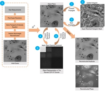 Abstract: My research focuses on the use of computation/algorithms to create new optical microscopy, sensing, and diagnostic techniques, significantly improving existing tools for probing micro‐ and nano‐objects while also simplifying the designs of these analysis tools. In this presentation, I will introduce a new set of computational microscopes which use lens‐free on‐chip imaging to replace traditional lenses with holographic reconstruction algorithms. Basically, 3D images of specimens are reconstructed from their “shadows” providing considerably improved field‐of‐view (FOV) and depth‐of‐field, thus enabling large sample volumes to be rapidly imaged, even at nanoscale. These new computational microscopes routinely generate >1–2 billion pixels (giga‐pixels), where even single viruses can be detected with a FOV that is >100 fold wider than other techniques. At the heart of this leapfrog performance lie self‐assembled liquid nano‐lenses that are computationally imaged on a chip. These self‐assembled nano‐lenses are stable for >1 hour at room temperature, and are composed of a biocompatible buffer that prevents nano‐particle aggregation while also acting as a spatial “phase mask.” The field‐of‐view of these computational microscopes is equal to the active‐area of the sensor‐array, easily reaching, for example, >20 mm2 or >10 cm2 by employing state‐of‐the‐art CMOS or CCD imaging chips, respectively. In addition to this remarkable increase in throughput, another major benefit of this technology is that it lends itself to fieldportable and cost‐effective designs which easily integrate with smartphones to conduct giga‐pixel tele‐pathology and microscopy even in resource‐poor and remote setings where traditional techniques are difficult to implement and sustain, thus opening the door to various telemedicine applications in global health. Some other examples of these smartphone‐based biomedical tools that I will describe include imaging flow cytometers, immunochromatographic diagnostic test readers, bacteria/pathogen sensors, blood analyzers for complete blood count, and allergen detectors. Through the development of similar computational imagers, I will also report the discovery of new 3D swimming patterns observed in human and animal sperm. One of this newly discovered and extremely rare motion is in the form of “chiral ribbons” where the planar swings of the sperm head occur on an osculating plane creating in some cases a helical ribbon and in some others a twisted ribbon. Shedding light onto the statistics and biophysics of various micro‐swimmers’ 3D motion, these results provide an important example of how biomedical imaging significantly benefits from emerging computational algorithms/theories, revolutionizing existing tools for observing various micro‐ and nano‐scale phenomena in innovative, high‐throughput, and yet cost‐effective ways. 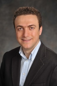 Biography: Dr. Aydogan Ozcan received his Ph.D. degree at Stanford University Electrical Engineering Department. After a short post‐doctoral fellowship at Stanford University, he was appointed as a research faculty at Harvard Medical School, Wellman Center for Photomedicine in 2006. Dr. Ozcan joined UCLA in the summer of 2007 as an Assistant Professor, and was promoted to Associate and Full Professor ranks in 2011 and 2013, respectively. He is currently the Chancellor’s Professor at UCLA and an HHMI Professor with the Howard Hughes Medical Institute, leading the Bio‐ and Nano‐Photonics Laboratory at UCLA Electrical Engineering and Bioengineering Departments, and is also the Associate Director of the California NanoSystems Institute (CNSI) at UCLA. Dr. Ozcan holds 32 issued patents (all of which are licensed) and more than 20 pending patent applications for his inventions in nanoscopy, wide‐field imaging, lensless imaging, nonlinear optics, fiber optics, and optical coherence tomography. Dr. Ozcan gave more than 250 invited talks and is also the author of one book, the co‐author of more than 400 peer reviewed research articles in major scientific journals and conferences. In addition, Dr. Ozcan is the founder and a member of the Board of Directors of Holomic LLC. Prof. Ozcan was selected as one of the top 10 innovators by the U.S. Department of State, USAID, NASA, and NIKE as part of the LAUNCH: Health Forum organized in 2010. He also received the 2012 World Technology Award on Health and Medicine, which is presented by the World Technology Network in association with TIME, CNN, AAAS, Science, Technology Review and Fortune. Dr. Ozcan is elected Fellow of SPIE and OSA, and is a Lifetime Member of AAAS. |
Mailing ListSupported ByThorlabs designs and produces a variety of optomechanical and optoelectronic components in 15 facilities around the globe. Thorlabs seeks to listen and serve its customers with over 20,000 products available.

Founded in 2018, Nexus Photonics has developed integrated photonics ready to scale. Smaller, lighter and faster, their platform outperforms industry benchmarks, and operates in an ultra-broadband wavelength range from ultraviolet to infrared to support a wide breadth of practical applications.
Archives
May 2024
Categories
All
|


