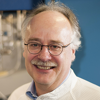
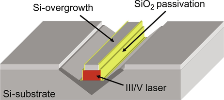
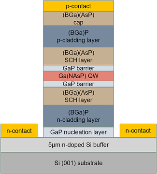
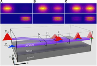
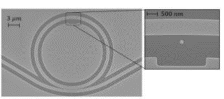
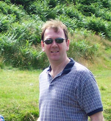
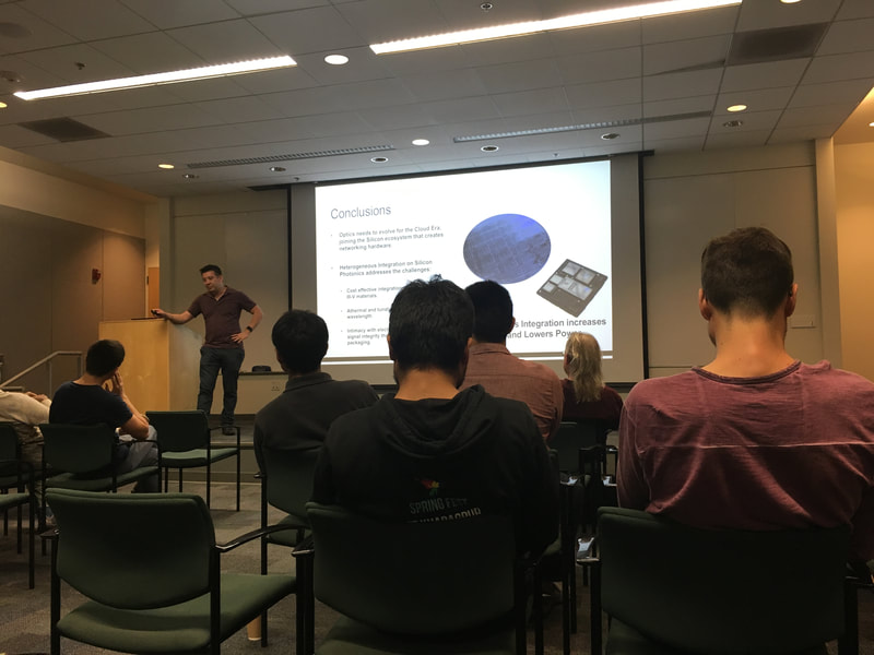
Friday July 21st, 1:00pm in Henley Hall 1010 In recent years, the monolithic integration of III/V-semiconductor materials and heterostructures on CMOS-compatible (001) Si-substrate is gaining increasing interest for the realization of novel integrated circuits with improved electronic, optoelectronic or photonic functionalities. The principal challenges of the III/V-material integration on CMOS-compatible (001) Si-substrates will be reviewed and possible solutions for the high-quality deposition of III/V-layer stacks will be demonstrated for large area 300 mm (001) Si-wafers by applying low-temperature metal organic vapour phase epitaxy (MOVPE) processes. Examples of successfully developed technologies including defect-free GaP-on-Si-template wafers as well as novel lattice-matched Ga(NAsP)-based laser stacks for Si-photonics applications will be presented and discussed. Wolfgang Stolz is full professor and co-head of the Structure and Technology Research Laboratory (Material Sciences Center and Faculty of Physics, Philipps-University Marburg (Germany)), Adjunct Professor at the Optical Sciences Center (University of Arizona, Tucson (USA)) and Chief Technology Officer (CTO NAsP III/V GmbH, Marburg (Germany)). His current fields of activities include the epitaxial growth for a wide range of III/V-compound semiconductor material systems and heterostructures by applying metal organic vapour phase epitaxy (MOVPE) as well as realization of novel device concepts for electronic, solar cell and laser applications in particular also monolithically integrated on CMOS-compatible (001) Si-substrates.
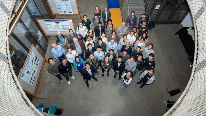
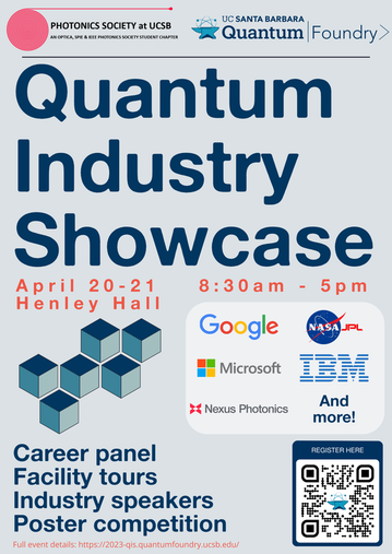
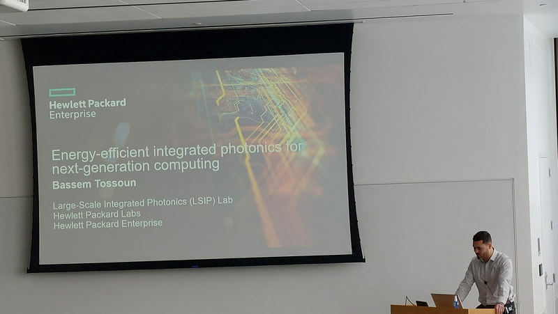
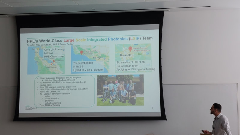
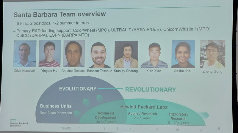
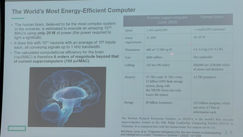
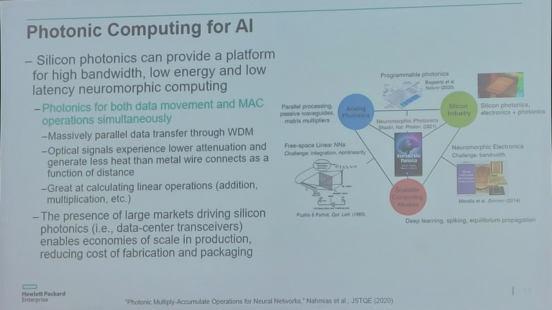
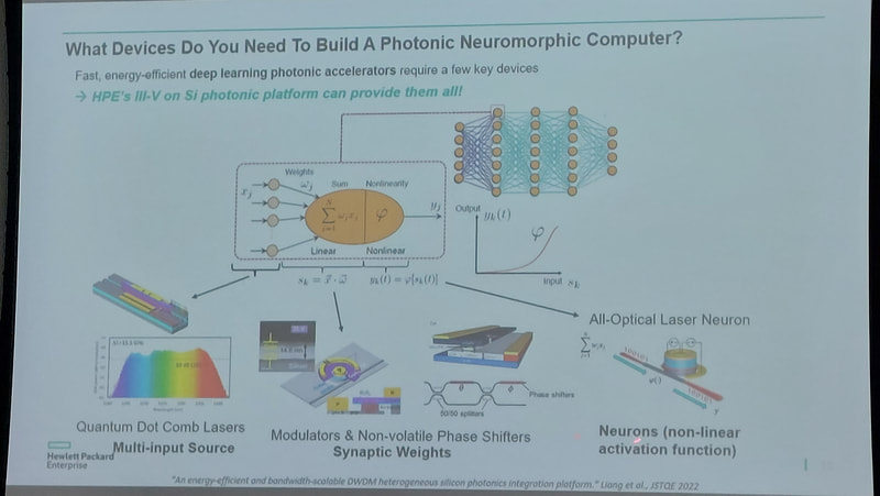
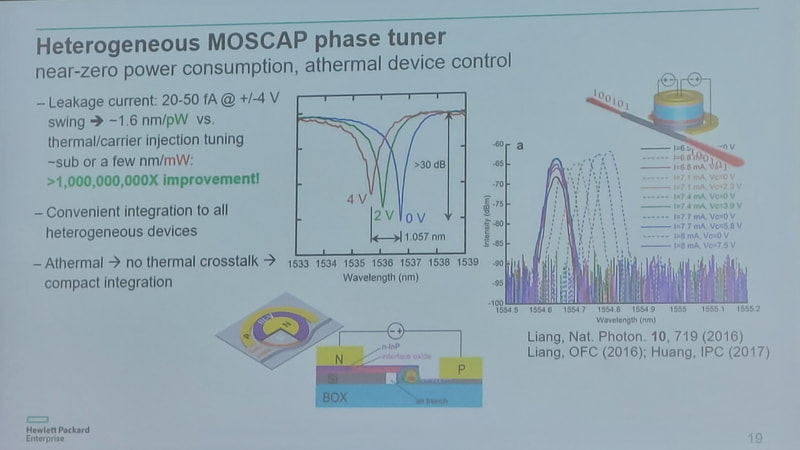
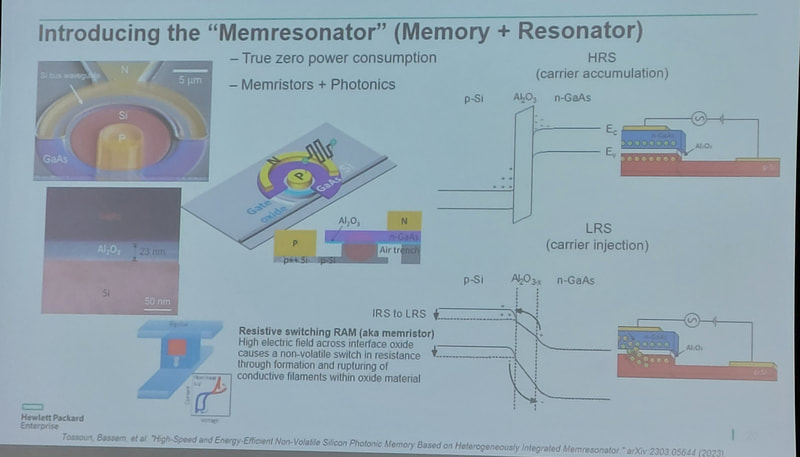
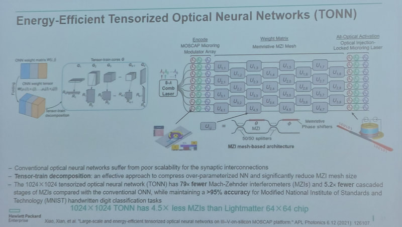
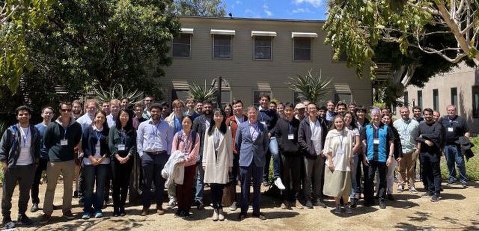
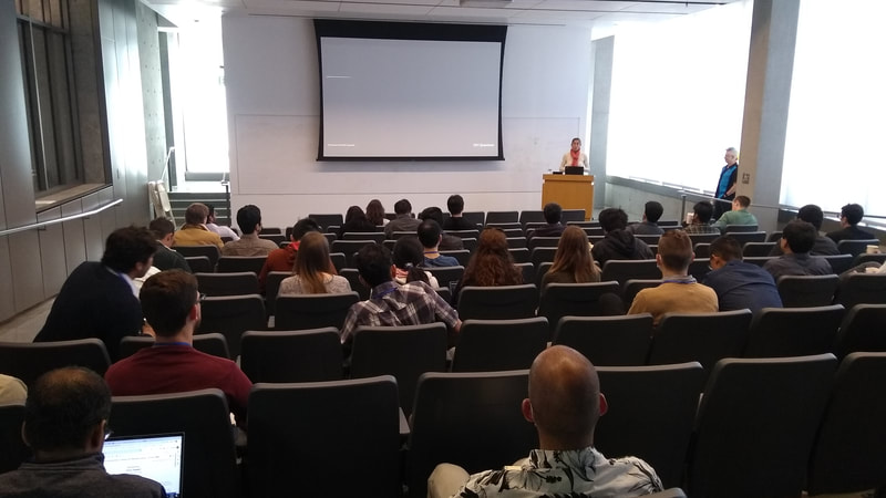
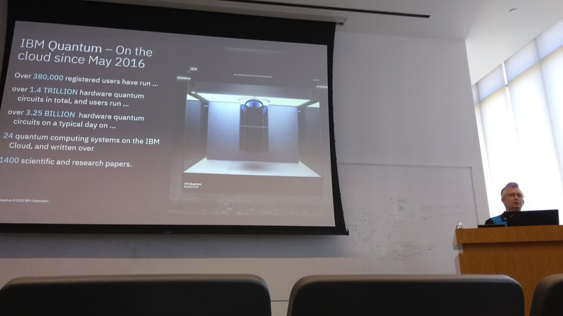
One day one, the keynote speaker, Monica Hansen from Google, delivered a engaging presentation on "Building a Useful Quantum Computer," shedding light on the challenges and breakthroughs in quantum computing. Following the keynote, attendees had the opportunity to attend a series of presentations from companies working in quantum. Tin Komljenovic from Nexus Photonics presented on "Heterogeneous Photonics for Quantum," exploring the use of photonics in quantum technologies. Das Pemmaraju from IBM discussed their advancements in "Moving Towards Practical Quantum Advantage with Scalable Quantum Computing." Garrett Cole from Thorlabs Crystalline Solutions introduced "Semiconductor Supermirrors for Quantum Optical Metrology," presenting the potential of supermirrors in quantum applications. After lunch, the event resumed with more engaging presentations. Kate Raach from HRL shared insights on "Encoded Silicon Qubits: A High-Performance & Scalable Platform for Quantum Computing." Makan Mohageg from NASA JPL discussed "Space-Based Quantum Technologies at JPL," unveiling their research endeavors in quantum-related projects. The company led sessions ended with a career panel, providing a platform for students to gain valuable industry insights from the panelists. The panel discussion shed light on career opportunities, challenges, and future prospects in the dynamic field of quantum information science. The day concluded with the student poster session where students were able to showcase their work and discuss with industry members and other attendees. Day 2 provided students with the opportunity to talk 1:1 to specific representatives during office hours and to visit the facilities of 3 local companies. Asylum/Oxford Instruments, Google, and Thorlabs Crystalline Solutions opened their doors offering valuable insights into their quantum research and development initiatives. Acknowledgments and Sponsorship: The 2023 QIS event was made possible through the generous support of sponsor organizations, including HRL Laboratories, Nexus Photonics, Oxford Instruments, and Thorlabs Crystalline Solutions. Their contributions played a vital role in creating a platform for knowledge sharing, collaboration, and innovation within the quantum information science community. For more information see - https://2023-qis.quantumfoundry.ucsb.edu/ Friday March 24th, 12:00 pm in Henley Hall 1010 New machine learning algorithms such as deep neural networks and the availability of large datasets have created a large drive towards new types of hardware capable of executing these algorithms with higher energy-efficiency. Recently, silicon photonics has emerged as a promising hardware platform for neuromorphic computing due to its inherent capability to process linear and non-linear operations and transmit a high bandwidth of data in parallel. At Hewlett Packard Labs, an energy-efficient dense-wavelength division multiplexing (DWDM) silicon photonics platform has been developed as the underlying foundation for innovative neuromorphic computing architectures. The latest research on our silicon photonic neuromorphic platform will be presented and discussed. Biography:
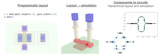
Bassem Tossoun received his PhD in Electrical Engineering at the University of Virginia in 2019 with his research interests including silicon photonics and the design, fabrication, and characterization of optoelectronic devices for data communications. Currently, he is a Senior Research Scientist at Hewlett Packard Labs working on heterogeneously integrated III-V on silicon photonic devices for next-generation optical computing and communications. GDSfactory is a design automation tool for photonics and analog circuits. You can describe your circuits with a code driven flow (python or YAML), verify them (DRC, simulation) and analyze them. Multiple Silicon Photonics foundries have gdsfactory PDKs available. In this tutorial on GDSfactory, you will learn: ●Define parametric cells (PCells) in python or YAML ●Define routes between components ●Test component settings, ports and geometry to avoid regressions
Abstract: As photonics matures beyond component-based devices, complex photonic integrated circuits are now being developed to meet commercial needs at the forefront of technology. Performance metrics are continually improved for lasers, modulators, multiplexers, detectors, and other important photonic components, but one capacity that has historically been challenging to scale is the optical wavelength. To develop a fully functional passive and active platform for wavelengths across the visible to near-IR brings additional challenges introduced by the various fabrication constraints of the different materials integrated on the same substrate. In this presentation Eric will discuss recent work on highly efficient nonlinear waveguides and on-going research to integrate a visible laser onto silicon chips with wide-band frequency conversion resonators. Next, he will motivate the need for improved performance of photonics to meet the demanding requirements for integrated quantum optics. Finally, a new application of nonlinear optics in the far-UVC for disinfection and Raman spectroscopy will be introduced. Bio: Eric Stanton attended Cal Poly San Luis Obispo, where he developed CubeSat nanosatellites and graduated with a B.Sc. in Electrical Engineering in 2012. During the summer of 2012 he worked at Agilent (now Keysight) before entering the graduate program at the University of California Santa Barbara (UCSB). In Professor John Bowers’ group, he developed integrated photonic technologies for a wide range of wavelengths from the visible to the mid-infrared. He obtained his Ph.D. in 2018 from the Electrical and Computer Engineering department at UCSB, and was awarded an NRC Postdoctoral Fellowship at the National Institute of Standards and Technology (NIST) in Boulder, CO. There he worked on nonlinear photonics and heterogeneously integrated lasers on silicon. Since 2020, he has been a CU Boulder PREP scientist at NIST. In 2021, he co-founded EMode Photonix, a photonics technology development company with the mission to make advanced photonic design tools more accessible. About Infinera Infinera is a global supplier of innovative open optical networking solutions that enable carriers, cloud operators, governments, and enterprises to scale network bandwidth, accelerate service innovation, and automate network operations. Infinera solutions deliver industry-leading economics and performance in long-haul, submarine, data center interconnect, and metro transport applications. To learn more about Infinera, visit www.infinera.com, follow on Twitter and LinkedIn, and subscribe for updates. Robert Maher Bio: Robert Maher, Ph.D. serves as Sr. Director and Head of the Optical Systems Group at Infinera. He has authored over 100 technical publications in the field of optical transmission technologies. He was awarded the Marie Curie Research Fellowship from the European Research Council (ERC) in 2010 and the University Research Fellowship from the Royal Society, UK, in 2016. In recognition of his technical contributions to the optical industry, he has been awarded Optica’s Paul F Foreman Team Engineering Excellence Award and the Colin Campbell Mitchell Award from the Royal Academy of Engineering (UK). In 2015, he was elevated to Senior Member of the IEEE. Dr. Maher holds a B.Eng. in Electronic Engineering and a Ph.D. in Electronic Engineering from Dublin City University, Ireland. Dave Welch Bio: David F. Welch, Ph.D. co-founded Infinera in 2001, and serves as Chief Innovation Officer and member of the Board of Directors. He holds over 130 patents in optical transmission technologies, and has authored over 300 technical publications in the same field. In recognition of his technical contributions to the optical industry, he has been awarded the OSA’s Adolph Lomb Medal, Joseph Fraunhofer Award and John Tyndall Award, the IET’s JJ Thompson Medal for Achievement in Electronics, and the IEEE Ernst Weber Managerial Leadership Award. He is a Fellow of the OSA and the IEEE. In 2016, he was elected to the National Academy of Engineering. Dr. Welch holds a B.S. in Electrical Engineering from the University of Delaware and a Ph.D. in Electrical Engineering from Cornell University. Event Summary:
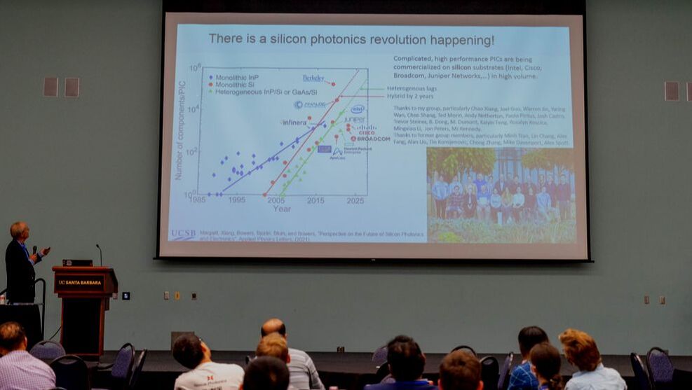
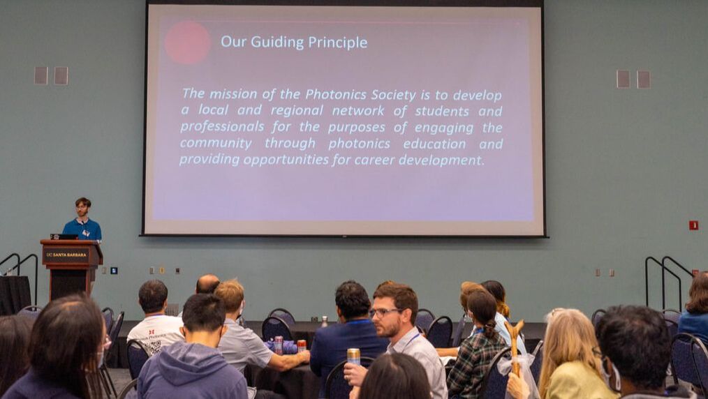
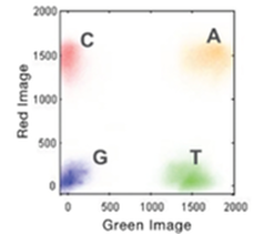
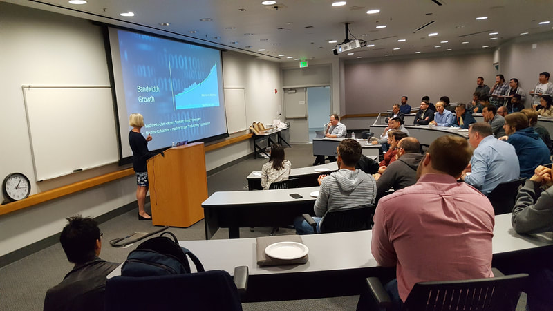
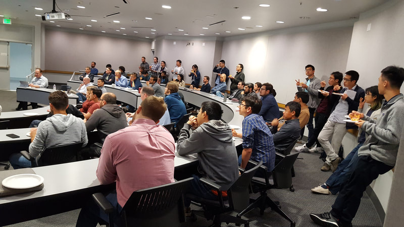
Dr. Robert Maher gave an overview of Infinera’s product solutions, the evolution of their coherent optical engine, and their latest ICE6 product. He discussed the integration of the electronic and photonic chips and the advantages of probabilistic constellation shaping for fine tuning the spectral efficiency for a given SNR. Dr. Dave Welch discussed the advantages of point-to-multipoint optical links in cost, flexibility, and network simplification. He described the operating principles of their XR Optics Transceiver in these optical links. 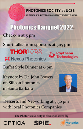 On Friday, May 27 at 5pm, graduate students, UCSB professors, and representatives from 10 local photonics companies gathered for a night of food and networking at the UCSB Corwin Pavilion. The Banquet began with a recruitment pitch for the Photonics Society followed by talks from Thorlabs, Nexus Photonics, and Raytheon Vision Systems who are all major sponsors of the Photonics Society this year. Thanks to their generous support, the photonics society was able to host this event and many other small events at no cost to attendees. After a bountiful dinner, Professor Bowers co-hosted a talk with all of the companies in attendance to provide an overview of all the photonics opportunities in Santa Barbara. The presentation slides from Thorlabs, Nexus Photonics, Raytheon Vision Systems, and Professor Bowers can be accessed here. In his talk, Bowers showed work from Quintessent, OpenLight (prev. Aurrion), Morton Photonics, OE Solutions, Aeluma, Freedom Photonics, Ultra-Low Loss Technologies, Mirios, and Nexus Photonics. During his talk he passed the microphone to several of the industry members from these companies, giving them a chance to talk about their work. Industry members were excited to be back in person for networking and several were actively hiring students at the event. Thanks again to our Sponsors and Parent Organizations!Learn more about our sponsors by viewing their presentation slides. Keynote Speaker - Dr. John BowersLearn more about Photonics in Santa Barbara by viewing the keynote presentation slides. 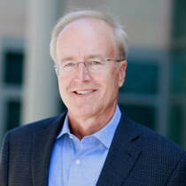 Dr. John Bowers is a world-leading researcher in the areas of silicon photonics, optoelectronics, energy efficiency and the development of novel low power optoelectronic devices for the next generation of optical networks. Dr. Bowers worked for AT&T Bell Laboratories and Honeywell before joining UC Santa Barbara. At UCSB, he holds the Fred Kavli Chair in Nanotechnology and is the Director of the Institute for Energy Efficiency and a Distinguished Professor in the Department of Electrical and Computer Engineering. His research interests include silicon photonics and integrated circuits, fiber optic networks, thermoelectrics, high efficiency solar cells, and optical switching. He is a cofounder of Aurrion, Aerius Photonics and Calient Networks. He has published two books, ten book chapters, 450 journal papers, 1000 conference papers and has received 54 patents. He and coworkers received the EE Times Annual Creativity in Electronics (ACE) Award for Most Promising Technology for the hybrid silicon laser in 2007. Member of : National Academy of Engineering, National Academy of Inventors Fellow of: Institute of Electrical and Electronics Engineers (IEEE), Optical Society of America (OSA), American Physical Society (APS), American Association for the Advancement of Science (AAAS) Honors: Nick Holonyak, Jr. Award, Optical Society (OSA); IEEE Photonics Award; Tyndall Award (OSA/IEEE ); IEEE LEOS William Streifer Award; International Conference on Indium Phosphide and Related Materials (IPRM) Award; Highly Cited Researchers List, Web of Science Group; South Coast Business and Technology's Entrepreneur of the Year Affiliations: American Institute for Manufacturing Integrated Photonics, Institute for Energy Efficiency Education: PhD Stanford University MS Stanford University Friday, May 13th, 1:00 pm (PST) -- pizza provided! Hosted in-person in ESB 1001 and via Zoom Bio – Alexa Hudnut is an Optical Systems Engineer at Illumina in San Diego. Her research background is true to a Biomedical Engineer – a little bit of everything. She started her research in molecular biology and gene editing and then worked her way to instrumentation design and optics. She graduated with a PhD in Biomedical Engineering from the University of Southern California in 2018. She is most passionate about creating medical devices that leverage Optics and Materials Science for an intentionally sustainable future. Abstract – Illumina’s mission is to improve human health by unlocking the power of the genome. This translates to efforts such as tracking COVID variants, determining your dog’s breed, population genomics, and everything in between. Next generation sequencing (NGS) relies heavily on epifluorescence microscopy as the backbone of instrumentation. As we look toward the future of gene sequencing, it will become more prevalent as an in vitro diagnostic (IVD). To improve the clinical workflow, increased throughput is necessary for quicker turnaround times. These improvements are being driven by innovations such as structured illumination, multiplexing, image processing, and nanofabrication. The Photonics Society collaborated with the UCSB NSF Quantum Foundry to host industry partners and students for an in-person showcase event on April 22, 2022.
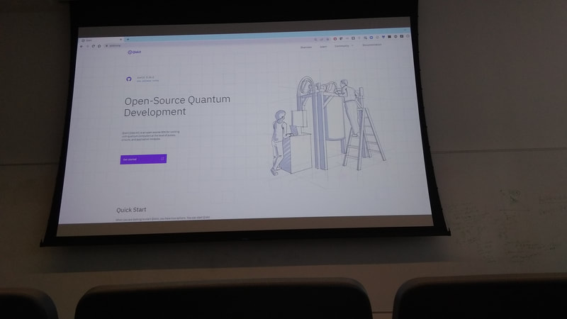
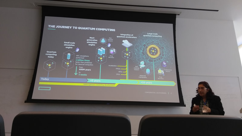
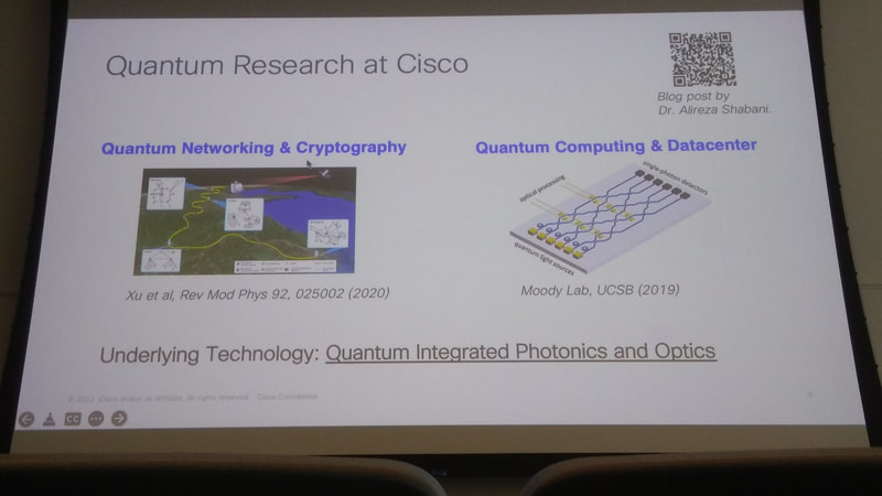
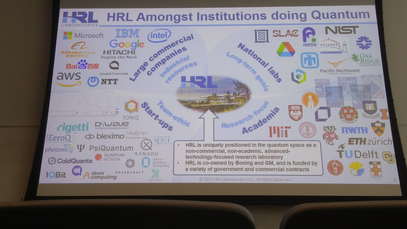
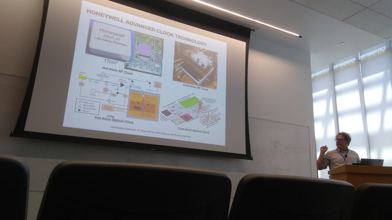
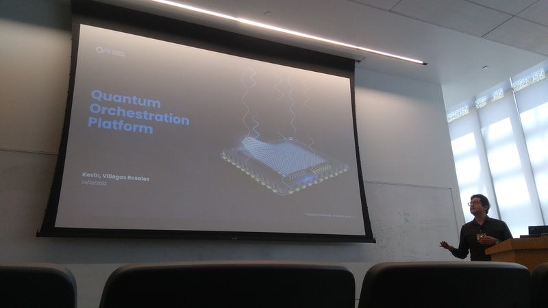
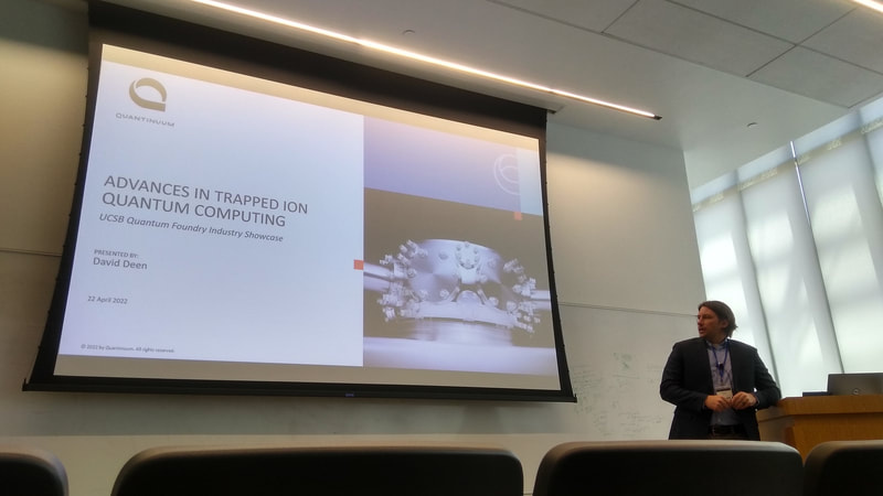
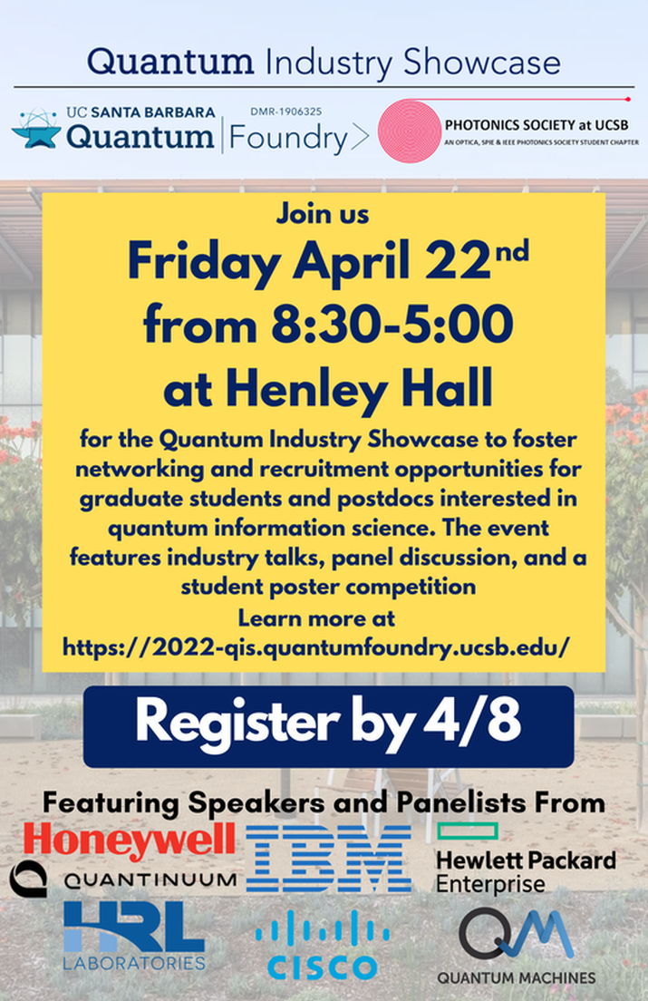
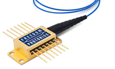
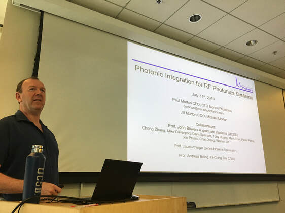
The goal of the Quantum Industry Showcase (QIS) is to connect industry partners with the graduate students and postdocs working in quantum materials and technologies. With opportunities to ask questions and chat in-person, the event helps to foster discussion, mentoring, and recruitment. The event began with a keynote given by Kevin Roche of IBM followed by presentations from Hewlett Packard Enterprise, Cisco, and HRL. Attendees were able to ask questions and chat with industry partners during a panel session and a networking lunch. In the afternoon, representatives from Honeywell, Quantum Machines, and Quantinuum gave presentations. The event concluded after giving students the opportunity to showcase their work at a poster session. The Quantum Industry Showcase was attended by industry partners from Thorlabs, Quantinuum, Oxford Instruments NanoScience, Bleximo, HRL, Hewlett Packard Enterprise, IBM, Quantum Machines, Cisco, Honeywell, and Nexus Photonics. Prior to the QIS event, Thorlabs provided students with a tour of their facilities. The QIS event was sponsored in part by Oxford Instruments. For more information, visit 2022-qis.quantumfoundry.ucsb.edu Thursday, November 18th, 11 am (PST) in Henley Hall 1010 Pizza will be provided! Cutting edge diode lasers and PICs for sensing applications Over the past several years, many new application areas for photonics in optical sensing have opened up. In this talk, we will review record performance diode laser and PIC technology developed by Freedom Photonics for a variety of optical sensing applications - gas sensing, atomic sensing and LIDAR. Basic skills for a good technical team leader Many engineers with advanced degrees end up leading high-impact technical teams, in pursuit of research, development or production. In this talk, we will discuss various practical issues related to being a good team leader. Wednesday, July 31 | 12:00pm | ESB 2001 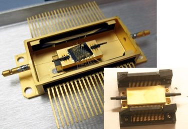 Photonic Integration for RF Photonics Systems Photonic integration on the Silicon Photonics platform, together with heterogeneous integration to include other materials, provides an ideal platform for the development of complex photonic integrated circuit (PIC) devices. This talk will describe the requirements for basic RF Photonics systems, including low noise lasers, linear modulators, low loss optical processing elements, and high power photodetectors, followed by descriptions of devices and PICs that Morton Photonics is developing for these functions. The talk will describe how a high performance PIC including arrays of these devices can be utilized for the processing of a phased array sensor to provide Multiple-Channel Simultaneous RF Beamforming, and describe potential commercial markets for these technologies, including automotive LIDAR systems, analog photonic links and RF Beamforming for 5G systems Refreshments Provided!
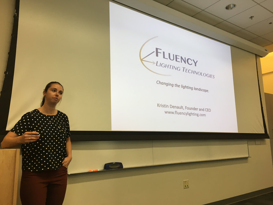
Friday, May 17th | 12:00 pm | ESB 2001 Fluency Lighting Technologies is an early stage start-up company developing technology out of UC Santa Barbara. At Fluency, we are creating next-generation bright and narrow-beam light sources for highly efficient illumination, using laser technology and materials design. Our focus is the development of low-cost, optical platforms that convert laser diode emission into high-quality white light in various light levels, beam angles, and color temperatures, designed for customer-driven metrics, in applications where energy-saving LED technology is not used because of the limited light output from an LED. Refreshments will be provided
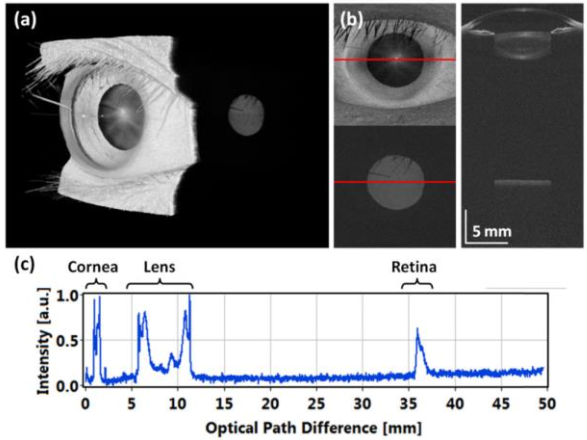
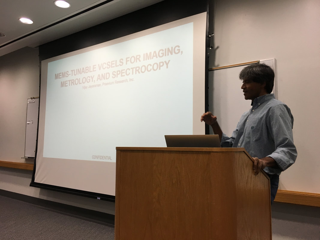
Thursday, May 16th | 12:00 pm | Elings 1601 In recent years, widely tunable micro-electro-mechanical systems vertical cavity surface-emitting lasers (MEMS-VCSELs) have found commercial application in swept source optical coherence tomography medical imaging and also show considerable promise in metrology and spectroscopy. These devices exhibit fractional tuning ranges of >11% of the center wavelength, wavelength tuning repetition rates over full tuning range of >1MHz, and clean single-mode operation. These properties, in conjunction with small size and wafer scale fabrication and testing, promise an economical optical source that can impact sensing applications from the visible to the mid-infrared. Refreshments will be provided
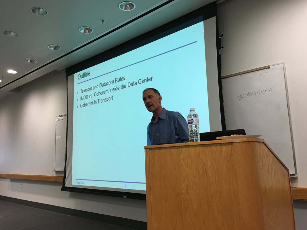
Thursday, May 9th | 12:00 pm | Elings 1601 Chris will discuss next-generation optical interfaces for large scale datacenters, including Intensity Modulated Direct Detection and Coherent technologies at 100, 200, 400 and 800 Gb/s rates. He will show several examples of how applying insights gained from previously successful applications can lead to flawed conclusions about different applications. If he is persuasive, students will no longer trust what they are taught by their professors and other experts. Refreshments Provided.
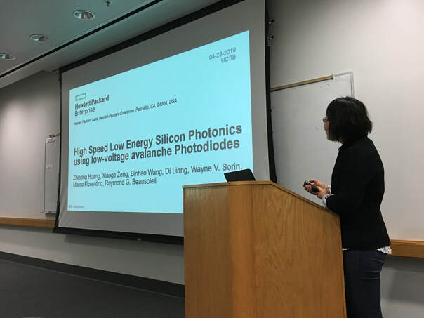
Tuesday, April 23rd | 12:00 pm | Elings 1601  Today zettabytes of data are generated and nearly doubled every two years. The conventional microprocessor is reaching its physical limitation and cannot keep up with the exponential growth in rich data. This leads to the increased demands on memory systems due to their frequent access patterns between microprocessors and memories. High speed, low energy and high sensitive optical data links are desirable for data transmission between multicores, microprocessors and memories in the new data center and high performance computer architectures. I am going to talk about the silicon photonics efforts in developing low energy high speed optical links in Hewlett Packard Labs, including the development of low voltage SiGe avalanche photodiodes, as well as photonic links. Refreshments Provided!
Monday, April 15 | 12:00pm | Elings 1605
Refreshments Provided!
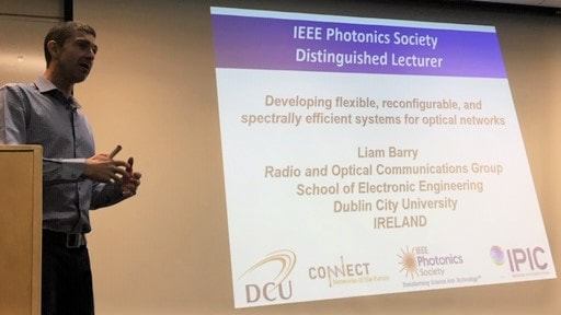
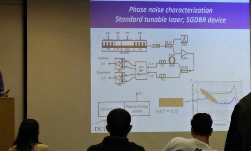
Monday March 11th, 11am, ESB 1001 Abstract The continuing growth in demand for bandwidth (from residential and business users), necessitates significant research into new advanced technologies that will be employed in future broadband communication systems. Two specific technologies, becoming increasingly important for future photonic systems, are wavelength tunable lasers and optical frequency combs. Although these topics have been studied for over two decades their significance for the development of future ultra-high capacity photonic systems has only recently been fully understood. Wavelength tunable lasers are currently becoming the norm in optical communication systems because of their flexibility and ability to work on any wavelength. However, as their operating principles are different to standard single mode lasers they can effect how future systems will operate. For example as optical transmission systems move towards more coherent transmission (where the data is carried using both the intensity and phase of the optical carrier), the phase noise in these tunable lasers will become increasingly important. Optical frequency combs also have many applications for future photonics systems, and for telecommunications they can be used to obtain the highest spectral efficiency in optical transmission systems by employing the technology of optical frequency division multiplexing (OFDM), and also for generation of high frequency RF signals in future 5G networks. Wavelength tunable lasers and optical frequency combs are thus topics at the leading edge of current photonics systems research, and their detailed understanding promises new applications in all-optical signal processing, optical sensing and metrology, and specifically telecommunications. This talk will focus on the development and characterization of various wavelength tunable lasers and optical frequency combs, and then outline how these sources can be employed for developing optical transmission systems and networks which make the best use of available optical spectrum. Biography Liam Barry received his BE (Electronic Engineering) and MEngSc (Optical Communications) degrees from University College Dublin in 1991 and 1993 respectively. From February 1993 until January 1996 he was employed as a Research Engineer in the Optical Systems Department of France Telecom's Research Laboratories (now known as Orange Labs) in Lannion, France, and as a result of this work he obtained his PhD Degree from the University of Rennes in France. In February 1996 he joined the Applied Optics Center in Auckland University, New Zealand, as a Research Fellow and in March 1998 he took up a lecturing position in the School of Electronic Engineering at Dublin City University, and established the Radio and Optical Communications Laboratory. From April 2006 until February 2010 he served as Director of The Rince Institute, an interdisciplinary research center with over 100 researchers. He is currently a Professor in the School of Electronic Engineering, a Principal Investigator for Science Foundation Ireland, and Director of the Radio and Optical Communications Laboratory. His main research interests are; all-optical signal processing, optical pulse generation and characterization, hybrid radio/fibre communication systems, wavelength tuneable lasers for reconfigurable optical networks, and optical performance monitoring. He has published over 200 articles in international peer reviewed journals, 250 papers in international peer reviewed conferences, and holds 10 patents in the area of optoelectronics. He has been a TPC member for the European Conference on Optical Communications (ECOC) since 2004, and a TPC member for the Optical Fibre Communication Conference (OFC) from 2007 to 2010, serving as Chair of the Optoelectronic Devices sub-committee for OFC 2010. Refreshments provided!
Thursday, Feb 28, 12 - 1 pm, ESB 1001
Refreshments will be provided
 Wednesday November 28th, 2 pm, ESB 1001 Alex is an entrepreneur with a track record of building teams that take ideas from the research laboratory through commercialization. Alex was a co-founder, the CEO, and Board Director of Aurrion from 2008-2016 which was a fabless semiconductor company that developed photonic integrated circuits for data center networking applications. The business was acquired by Juniper Networks. Alex worked for IBM, Lawrence Livermore National Laboratory, and Intel prior to founding Aurrion. Alex earned his M.S & Ph.D. from UCSB and is an alumnus of the Harvard Business School Owner/President Management Program. In his downtime, Alex enjoys riding off road motorcycles, playing guitar, smoking meat and reading books. Alex loves spending time with his wife and daughter going to live shows, travelling and eating weird stuff. Refreshments Provided!
|
Mailing ListSupported ByThorlabs designs and produces a variety of optomechanical and optoelectronic components in 15 facilities around the globe. Thorlabs seeks to listen and serve its customers with over 20,000 products available.

Founded in 2018, Nexus Photonics has developed integrated photonics ready to scale. Smaller, lighter and faster, their platform outperforms industry benchmarks, and operates in an ultra-broadband wavelength range from ultraviolet to infrared to support a wide breadth of practical applications.
Archives
May 2024
Categories
All
|


