|
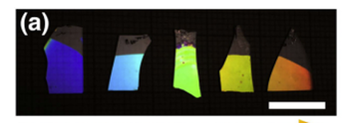
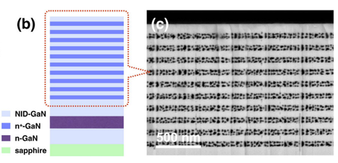
Friday March 4th at 1:00pm PST in Henley Hall 1010 and via Zoom Pizza Provided in-person! Porous semiconducting nitrides are effectively a new class of semiconducting material, with properties distinct from the monolithic nitride layers from which devices from light emitting diodes (LEDs) to high electron mobility transistors are increasingly made. The introduction of porosity provides new opportunities to engineer a range of properties including refractive index, thermal and electrical conductivity, stiffness and piezoelectricity. Quantum structures may be created within porous architectures and novel composites may be created via the infiltration of other materials into porous nitride frameworks. A key example of the application of porous nitrides in photonics is the fabrication of high reflectivity distributed Bragg reflectors (DBRs) from alternating layers of porous and non-porous GaN. These reflectors are fabricated from epitaxial structures consisting of alternating doped and undoped layers, in which only the conductive, doped layers are electrochemically etched. Conventionally, trenches are formed using a dry-etching process, penetrating through the multilayer, and the electrochemical etch then proceeds laterally from the trench sidewalls. The need for these trenches then limits the device designs and manufacturing processes within which the resulting reflectors can be used. We have developed a novel alternative etching process, which removes the requirement for the dry-etched trenches, with etching proceeding vertically from the top surface through channels formed at naturally-occurring defects in the crystal structure of GaN. This etch process leaves an undoped top surface layer almost unaltered and suitable for further epitaxy. This new defect-based etching process provides great flexibility for the creation of a variety of sub-surface porous architectures on top of which a range of devices may be grown. Whilst DBR structures enable improved light extraction from LEDs and the formation of resonant cavities for lasers and single photon sources, recent development also suggest that thick, subs-surface porous layers may enable strain relaxation to help improve the efficiency of red microLEDs for augmented reality displays. Meanwhile, the option of filling pores in nitride layers with other materials provides new opportunities for the integration of nitrides with emerging photonic materials, such as the hybrid-perovskite semiconductors, with perovskites encapsulated in porous nitride layers demonstrating greatly improved robustness against environmental degradation. Comments are closed.
|
Mailing ListSupported ByThorlabs designs and produces a variety of optomechanical and optoelectronic components in 15 facilities around the globe. Thorlabs seeks to listen and serve its customers with over 20,000 products available.

Founded in 2018, Nexus Photonics has developed integrated photonics ready to scale. Smaller, lighter and faster, their platform outperforms industry benchmarks, and operates in an ultra-broadband wavelength range from ultraviolet to infrared to support a wide breadth of practical applications.
Archives
May 2024
Categories
All
|


