|
|
|
|
|
|
|
|

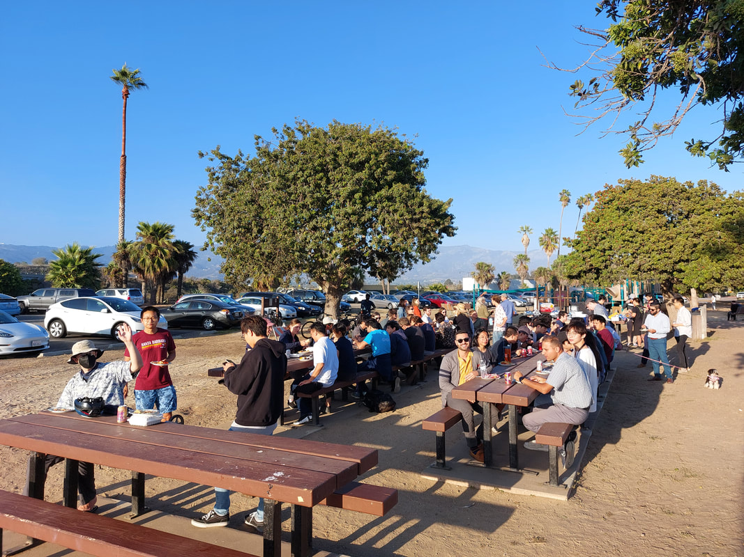
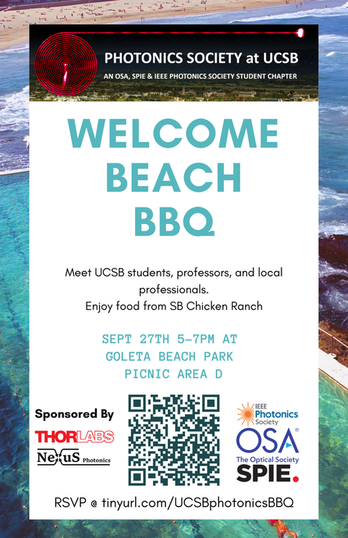
GDSfactory is a design automation tool for photonics and analog circuits. You can describe your circuits with a code driven flow (python or YAML), verify them (DRC, simulation) and analyze them. Multiple Silicon Photonics foundries have gdsfactory PDKs available. In this tutorial on GDSfactory, you will learn: ●Define parametric cells (PCells) in python or YAML ●Define routes between components ●Test component settings, ports and geometry to avoid regressions 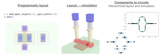 Students, professors, research staff, and industry professionals gathered at Goleta Beach Area D to catch up, talk about photonics, and make new connections while enjoying excellent food. The brisket and pork shoulder from Prof. Schow was the highlight of the event. There was good conversation with industry members from Nexus Photonics, Freedom Photonics, Quintessent, HPE, and Praevium. Newer students got a chance to interact with current grad students and industry. Wendy Ibsen talked about outreach opportunities. The event was a great success with approximately 70 attendees. 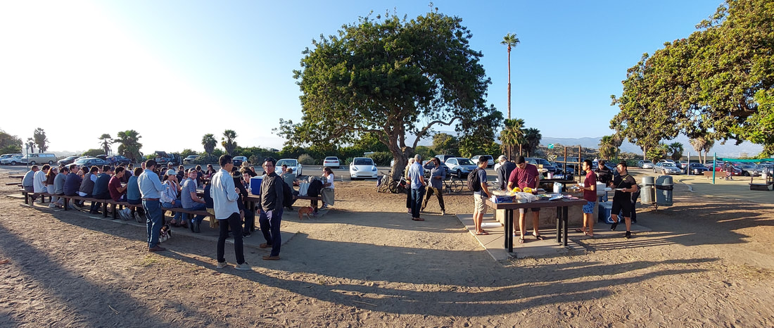 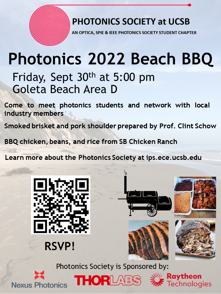 
Abstract: As photonics matures beyond component-based devices, complex photonic integrated circuits are now being developed to meet commercial needs at the forefront of technology. Performance metrics are continually improved for lasers, modulators, multiplexers, detectors, and other important photonic components, but one capacity that has historically been challenging to scale is the optical wavelength. To develop a fully functional passive and active platform for wavelengths across the visible to near-IR brings additional challenges introduced by the various fabrication constraints of the different materials integrated on the same substrate. In this presentation Eric will discuss recent work on highly efficient nonlinear waveguides and on-going research to integrate a visible laser onto silicon chips with wide-band frequency conversion resonators. Next, he will motivate the need for improved performance of photonics to meet the demanding requirements for integrated quantum optics. Finally, a new application of nonlinear optics in the far-UVC for disinfection and Raman spectroscopy will be introduced. Bio: Eric Stanton attended Cal Poly San Luis Obispo, where he developed CubeSat nanosatellites and graduated with a B.Sc. in Electrical Engineering in 2012. During the summer of 2012 he worked at Agilent (now Keysight) before entering the graduate program at the University of California Santa Barbara (UCSB). In Professor John Bowers’ group, he developed integrated photonic technologies for a wide range of wavelengths from the visible to the mid-infrared. He obtained his Ph.D. in 2018 from the Electrical and Computer Engineering department at UCSB, and was awarded an NRC Postdoctoral Fellowship at the National Institute of Standards and Technology (NIST) in Boulder, CO. There he worked on nonlinear photonics and heterogeneously integrated lasers on silicon. Since 2020, he has been a CU Boulder PREP scientist at NIST. In 2021, he co-founded EMode Photonix, a photonics technology development company with the mission to make advanced photonic design tools more accessible.

About Infinera Infinera is a global supplier of innovative open optical networking solutions that enable carriers, cloud operators, governments, and enterprises to scale network bandwidth, accelerate service innovation, and automate network operations. Infinera solutions deliver industry-leading economics and performance in long-haul, submarine, data center interconnect, and metro transport applications. To learn more about Infinera, visit www.infinera.com, follow on Twitter and LinkedIn, and subscribe for updates. Robert Maher Bio: Robert Maher, Ph.D. serves as Sr. Director and Head of the Optical Systems Group at Infinera. He has authored over 100 technical publications in the field of optical transmission technologies. He was awarded the Marie Curie Research Fellowship from the European Research Council (ERC) in 2010 and the University Research Fellowship from the Royal Society, UK, in 2016. In recognition of his technical contributions to the optical industry, he has been awarded Optica’s Paul F Foreman Team Engineering Excellence Award and the Colin Campbell Mitchell Award from the Royal Academy of Engineering (UK). In 2015, he was elevated to Senior Member of the IEEE. Dr. Maher holds a B.Eng. in Electronic Engineering and a Ph.D. in Electronic Engineering from Dublin City University, Ireland. Dave Welch Bio: David F. Welch, Ph.D. co-founded Infinera in 2001, and serves as Chief Innovation Officer and member of the Board of Directors. He holds over 130 patents in optical transmission technologies, and has authored over 300 technical publications in the same field. In recognition of his technical contributions to the optical industry, he has been awarded the OSA’s Adolph Lomb Medal, Joseph Fraunhofer Award and John Tyndall Award, the IET’s JJ Thompson Medal for Achievement in Electronics, and the IEEE Ernst Weber Managerial Leadership Award. He is a Fellow of the OSA and the IEEE. In 2016, he was elected to the National Academy of Engineering. Dr. Welch holds a B.S. in Electrical Engineering from the University of Delaware and a Ph.D. in Electrical Engineering from Cornell University. Event Summary:
Dr. Robert Maher gave an overview of Infinera’s product solutions, the evolution of their coherent optical engine, and their latest ICE6 product. He discussed the integration of the electronic and photonic chips and the advantages of probabilistic constellation shaping for fine tuning the spectral efficiency for a given SNR. Dr. Dave Welch discussed the advantages of point-to-multipoint optical links in cost, flexibility, and network simplification. He described the operating principles of their XR Optics Transceiver in these optical links. Quantum wells in Nanowires for Optoelectronic Applications: Materials and Devices - Dr. Lan Fu6/15/2022
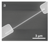
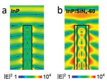
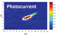
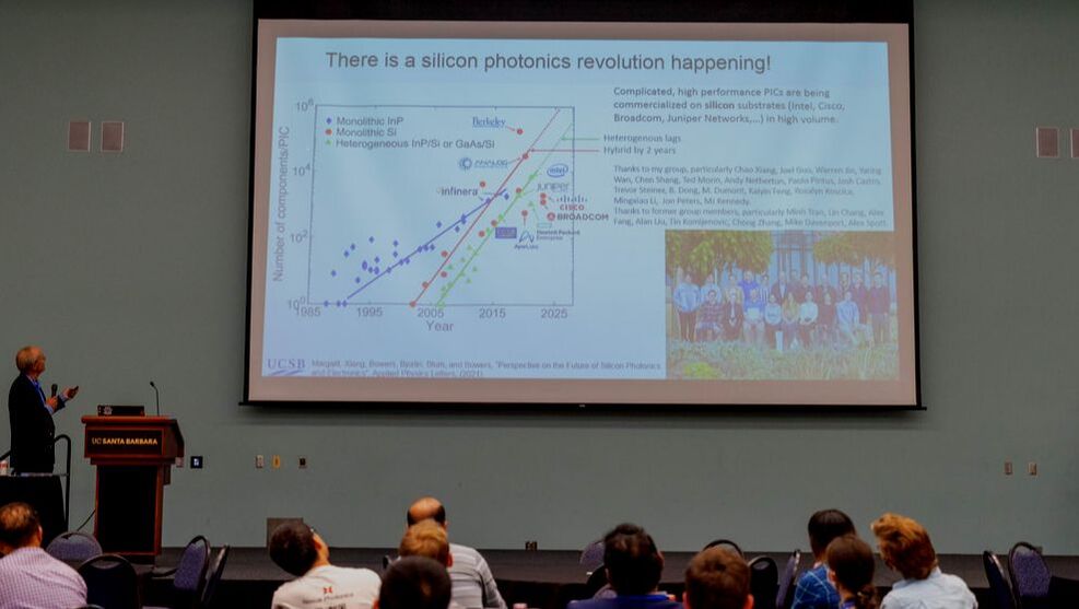
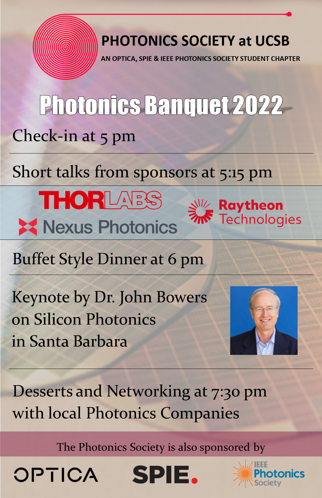
Thursday, June 23rd, 2:00 pm (PDT) -- Burgers from Kyle’s! Hosted in-person in Henley Hall 1010 Abstract – III-V compound semiconductor nanowires (NWs) have drawn much attention as nanoscale building blocks for integrated photonics/optoelectronics due to their nanoscale size, excellent optical properties and effectiveness in strain relaxation enabling the monolithic growth on lattice-mismatched substrates. In particular, NWs grown by selective area epitaxy technique have many advantages such as controllability of their size and position, high uniformity in diameter and length, as well as complementary metal-oxide-semiconductor (CMOS) process compatibility, facilitating their integration with other electronic devices. With suitable wavelength ranging from 1.3 to 1.6 μm and lattice match of constituent materials, InGaAs/InP quantum well (QW) has been being widely used for optical communication devices. However there has been limited understanding on the growth of InGaAs/InP QW in nanowire architecture and their application for optoelectronic devices such as lasers/LEDs and photodetectors. In this work, we present the study of the selective area epitaxy growth of InGaAs/InP multi-QW NW array by metalorganic chemical vapour deposition (MOCVD) technique, and the demonstration of nanowire LEDs/lasers and photodetectors with an investigation of their strong geometry related device properties by both numerical simulation and optoelectronic characterizations. Bio – Lan Fu received her PhD degree from the Australia National University (ANU) in 2001 and is currently a Full Professor at the Research School of Physics, ANU. Prof. Lan Fu was the recipient of the IEEE Photonic Society Graduate Student Fellowship (2000), Australian Research Council (ARC) Postdoctoral Fellowship (2002), ARF/QEII Fellowship (2005) and Future Fellowship (2012). Professor Fu is a senior member of IEEE, IEEE/Photonics and Electron Devices Societies and was the past chair of the Photonics Society, Electron Devices Society and Nanotechnology Council Chapters of the IEEE ACT section. She is the Chair of IEEE Nanotechnology Council Chapters & Regional Activities Committee, Associate Editor of IEEE Photonics Journal, and member of Editorial Board of Opto-Electronic Advances. She also the current member of the Australian Academy of Science National Committee on Materials Science and Engineering, Secretary of the Executive Committee of Australian Materials Research Society (AMRS), and Australian Research Council College of Experts. Professor Lan Fu’s main research interests include design, fabrication and integration of optoelectronic devices (LEDs, lasers, photodetectors and solar cells) based on low-dimensional III-V compound semiconductor structures including quantum wells, self-assembled quantum dots and nanowires grown by metal-organic chemical vapour deposition (MOCVD). Li, Z. Y., Tan, H. H., Jagadish, C., Fu, L., Adv. Mater. Technol. 2018, 3, 1800005. https://doi.org/10.1002/admt.201800005  On Friday, May 27 at 5pm, graduate students, UCSB professors, and representatives from 10 local photonics companies gathered for a night of food and networking at the UCSB Corwin Pavilion. The Banquet began with a recruitment pitch for the Photonics Society followed by talks from Thorlabs, Nexus Photonics, and Raytheon Vision Systems who are all major sponsors of the Photonics Society this year. Thanks to their generous support, the photonics society was able to host this event and many other small events at no cost to attendees. After a bountiful dinner, Professor Bowers co-hosted a talk with all of the companies in attendance to provide an overview of all the photonics opportunities in Santa Barbara. The presentation slides from Thorlabs, Nexus Photonics, Raytheon Vision Systems, and Professor Bowers can be accessed here. In his talk, Bowers showed work from Quintessent, OpenLight (prev. Aurrion), Morton Photonics, OE Solutions, Aeluma, Freedom Photonics, Ultra-Low Loss Technologies, Mirios, and Nexus Photonics. During his talk he passed the microphone to several of the industry members from these companies, giving them a chance to talk about their work. Industry members were excited to be back in person for networking and several were actively hiring students at the event. Thanks again to our Sponsors and Parent Organizations!Learn more about our sponsors by viewing their presentation slides.
Keynote Speaker - Dr. John BowersLearn more about Photonics in Santa Barbara by viewing the keynote presentation slides.  Dr. John Bowers is a world-leading researcher in the areas of silicon photonics, optoelectronics, energy efficiency and the development of novel low power optoelectronic devices for the next generation of optical networks. Dr. Bowers worked for AT&T Bell Laboratories and Honeywell before joining UC Santa Barbara. At UCSB, he holds the Fred Kavli Chair in Nanotechnology and is the Director of the Institute for Energy Efficiency and a Distinguished Professor in the Department of Electrical and Computer Engineering. His research interests include silicon photonics and integrated circuits, fiber optic networks, thermoelectrics, high efficiency solar cells, and optical switching. He is a cofounder of Aurrion, Aerius Photonics and Calient Networks. He has published two books, ten book chapters, 450 journal papers, 1000 conference papers and has received 54 patents. He and coworkers received the EE Times Annual Creativity in Electronics (ACE) Award for Most Promising Technology for the hybrid silicon laser in 2007.
Member of : National Academy of Engineering, National Academy of Inventors Fellow of: Institute of Electrical and Electronics Engineers (IEEE), Optical Society of America (OSA), American Physical Society (APS), American Association for the Advancement of Science (AAAS) Honors: Nick Holonyak, Jr. Award, Optical Society (OSA); IEEE Photonics Award; Tyndall Award (OSA/IEEE ); IEEE LEOS William Streifer Award; International Conference on Indium Phosphide and Related Materials (IPRM) Award; Highly Cited Researchers List, Web of Science Group; South Coast Business and Technology's Entrepreneur of the Year Affiliations: American Institute for Manufacturing Integrated Photonics, Institute for Energy Efficiency Education: PhD Stanford University MS Stanford University 
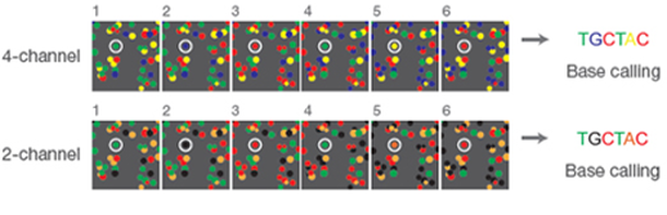
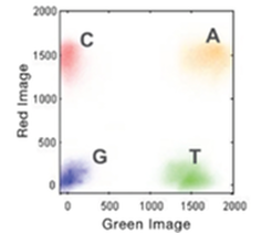
Friday, May 13th, 1:00 pm (PST) -- pizza provided! Hosted in-person in ESB 1001 and via Zoom Bio – Alexa Hudnut is an Optical Systems Engineer at Illumina in San Diego. Her research background is true to a Biomedical Engineer – a little bit of everything. She started her research in molecular biology and gene editing and then worked her way to instrumentation design and optics. She graduated with a PhD in Biomedical Engineering from the University of Southern California in 2018. She is most passionate about creating medical devices that leverage Optics and Materials Science for an intentionally sustainable future. Abstract – Illumina’s mission is to improve human health by unlocking the power of the genome. This translates to efforts such as tracking COVID variants, determining your dog’s breed, population genomics, and everything in between. Next generation sequencing (NGS) relies heavily on epifluorescence microscopy as the backbone of instrumentation. As we look toward the future of gene sequencing, it will become more prevalent as an in vitro diagnostic (IVD). To improve the clinical workflow, increased throughput is necessary for quicker turnaround times. These improvements are being driven by innovations such as structured illumination, multiplexing, image processing, and nanofabrication.
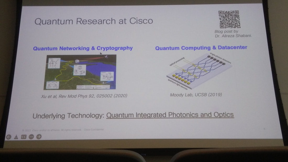
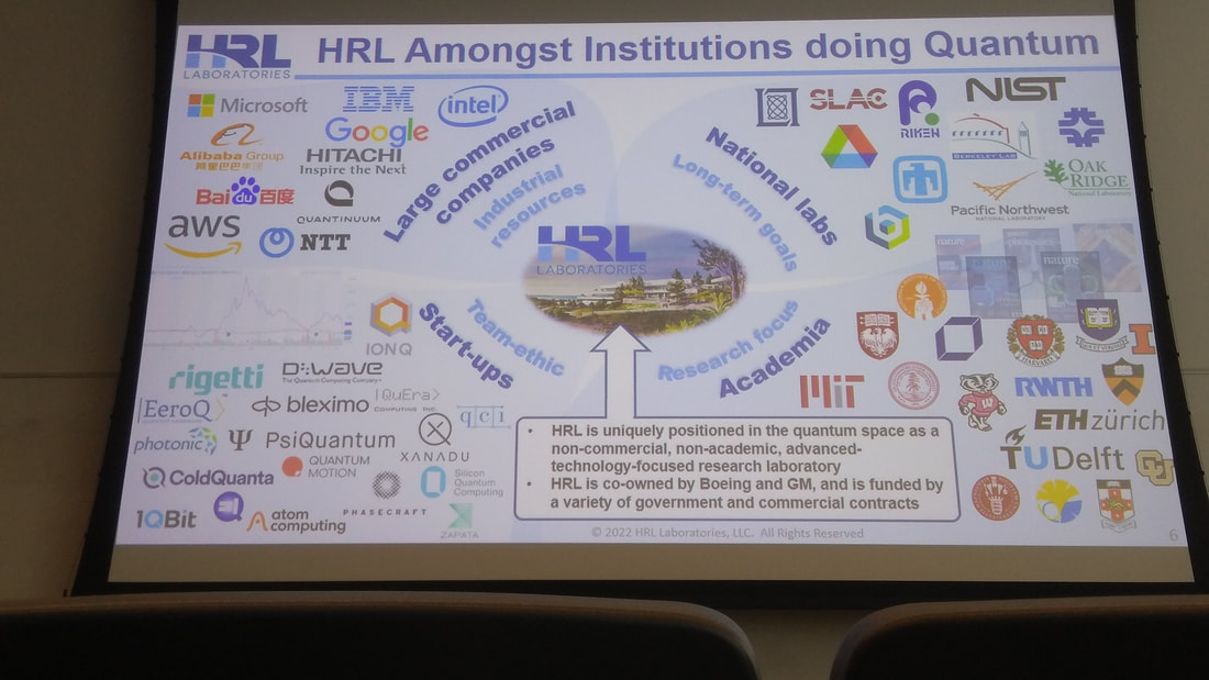
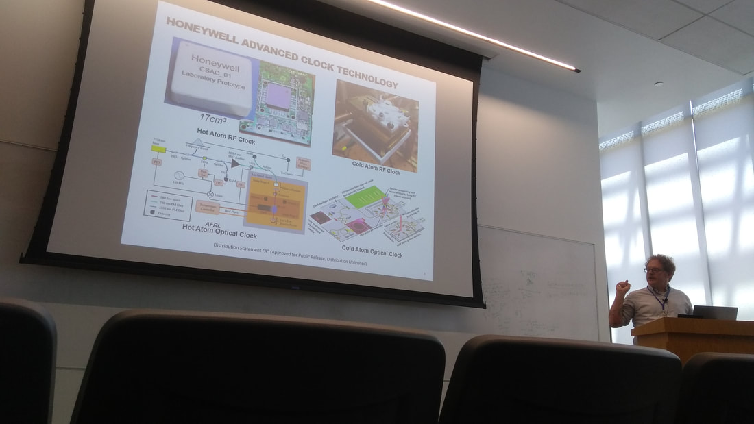
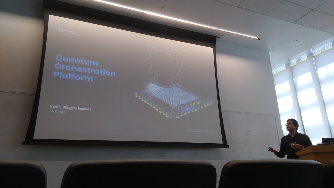
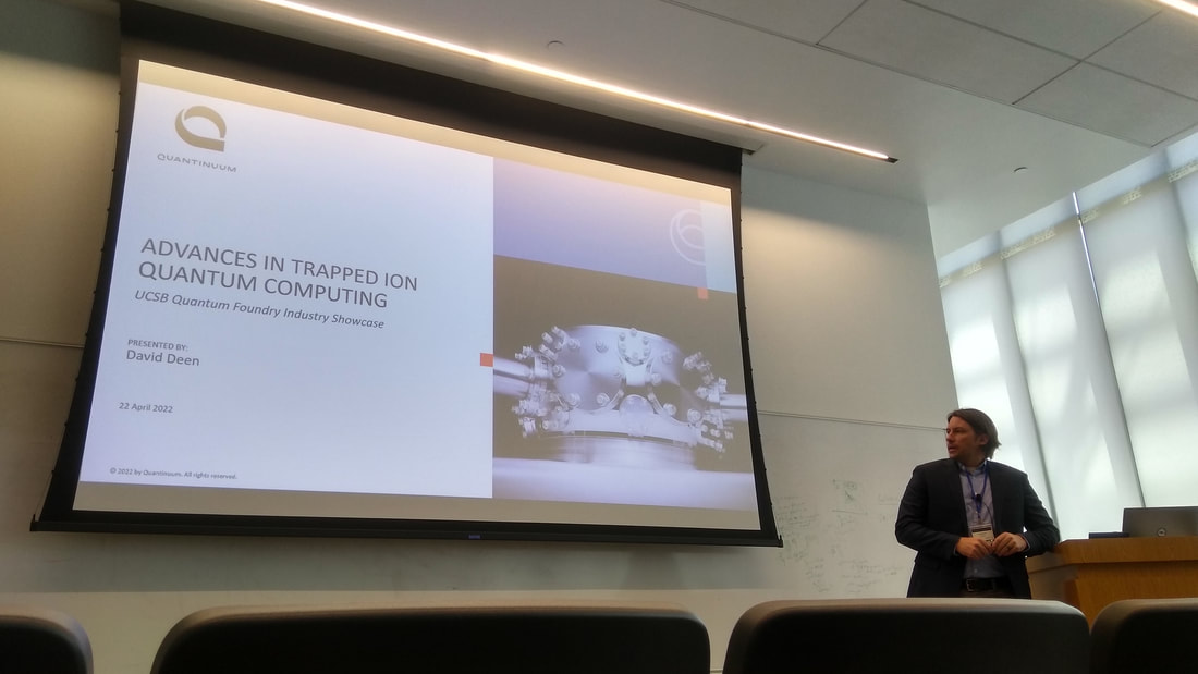
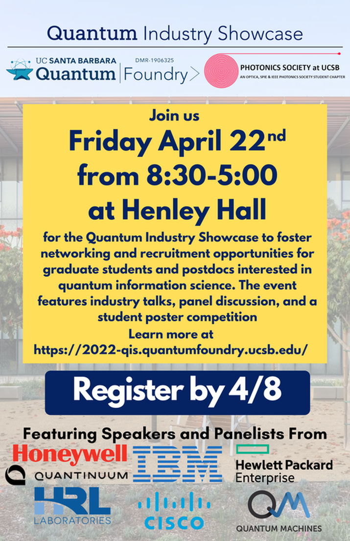
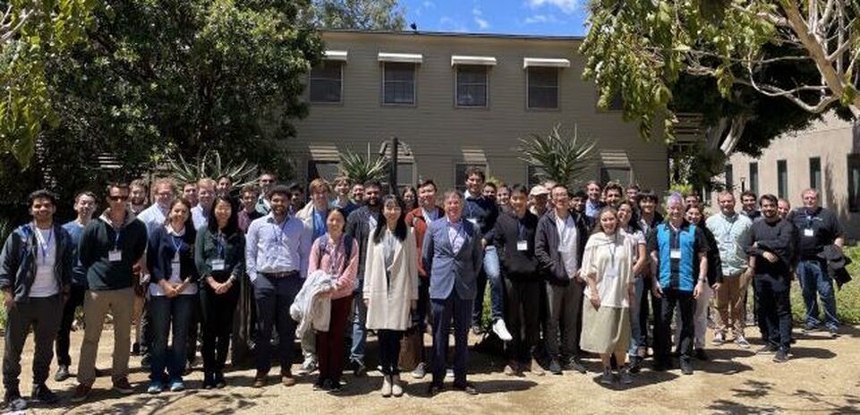 Group photo of the QIS 2022 attendees outside Henley Hall The Photonics Society collaborated with the UCSB NSF Quantum Foundry to host industry partners and students for an in-person showcase event on April 22, 2022. The goal of the Quantum Industry Showcase (QIS) is to connect industry partners with the graduate students and postdocs working in quantum materials and technologies. With opportunities to ask questions and chat in-person, the event helps to foster discussion, mentoring, and recruitment. The event began with a keynote given by Kevin Roche of IBM followed by presentations from Hewlett Packard Enterprise, Cisco, and HRL. Attendees were able to ask questions and chat with industry partners during a panel session and a networking lunch. In the afternoon, representatives from Honeywell, Quantum Machines, and Quantinuum gave presentations. The event concluded after giving students the opportunity to showcase their work at a poster session. The Quantum Industry Showcase was attended by industry partners from Thorlabs, Quantinuum, Oxford Instruments NanoScience, Bleximo, HRL, Hewlett Packard Enterprise, IBM, Quantum Machines, Cisco, Honeywell, and Nexus Photonics. Prior to the QIS event, Thorlabs provided students with a tour of their facilities. The QIS event was sponsored in part by Oxford Instruments. For more information, visit 2022-qis.quantumfoundry.ucsb.edu
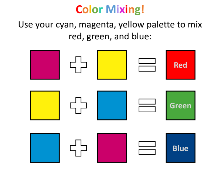
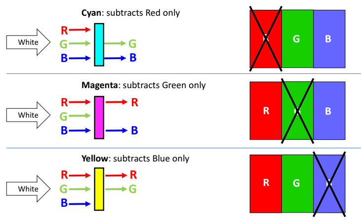
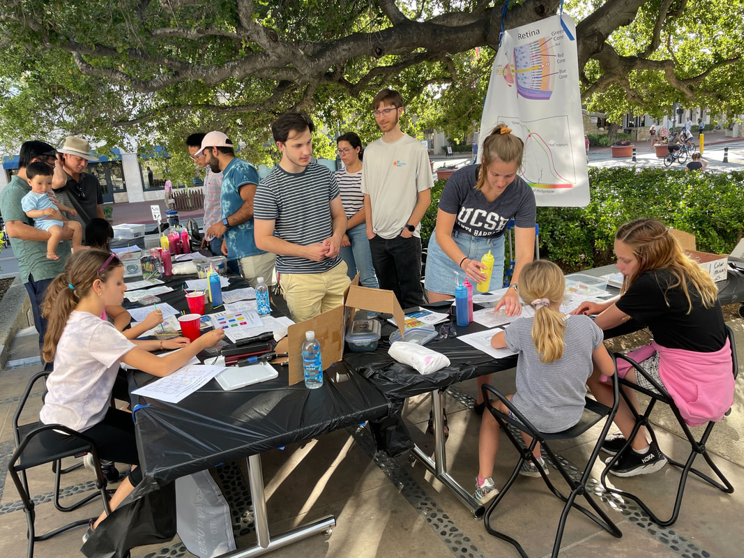
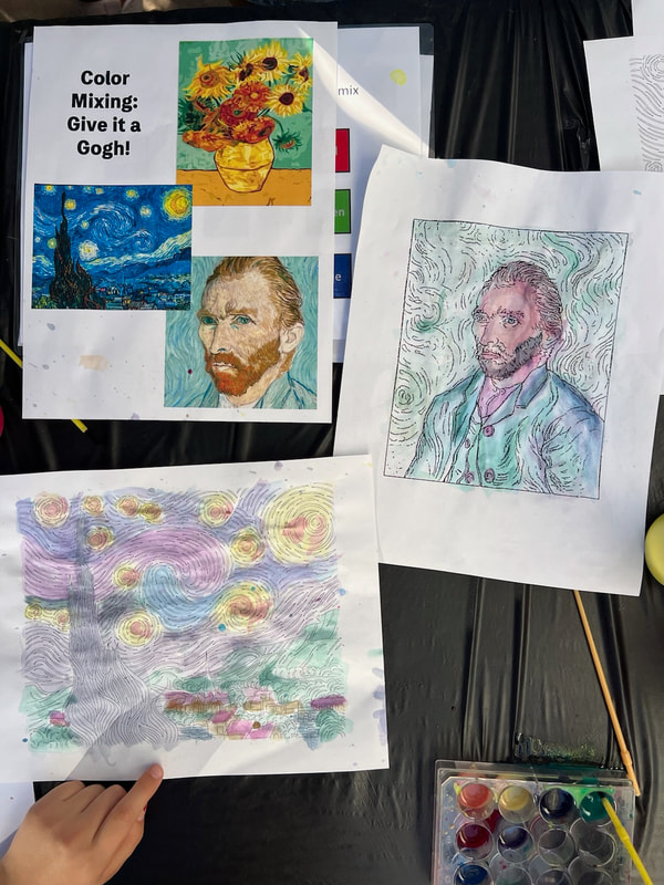
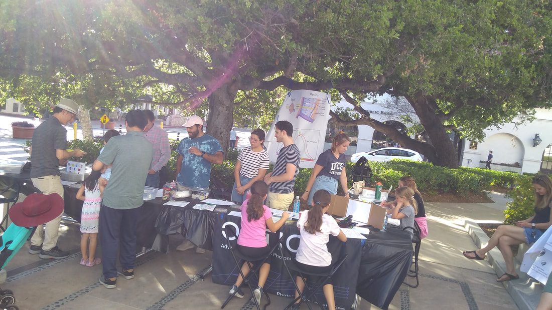
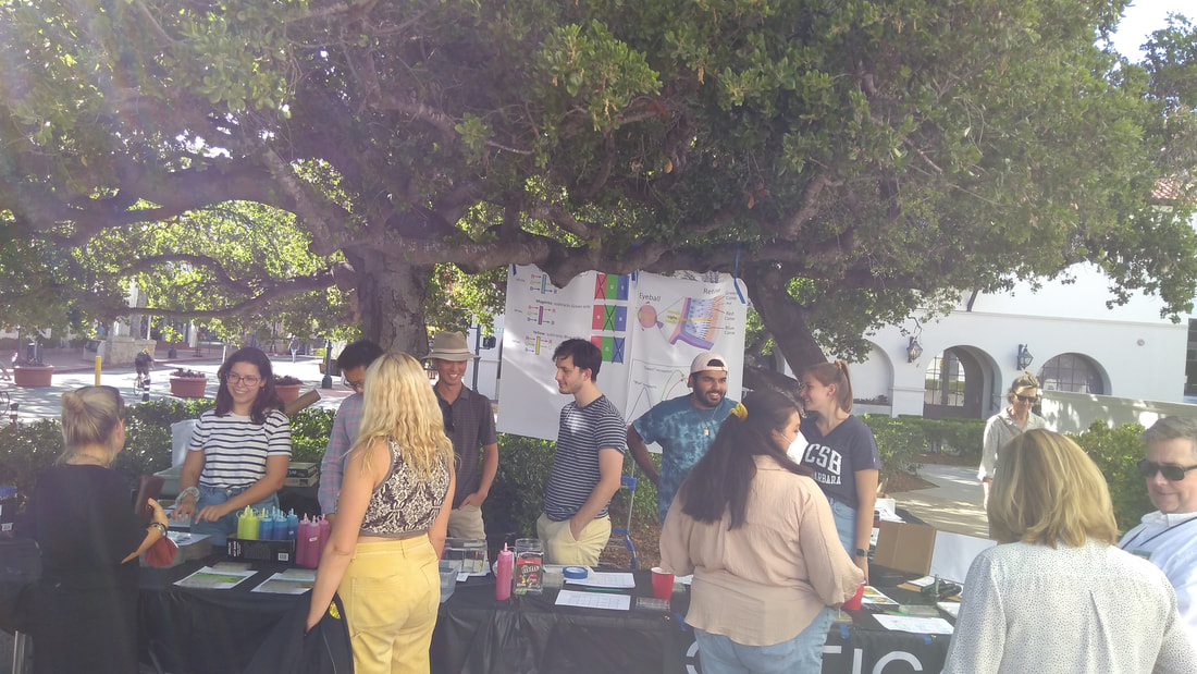
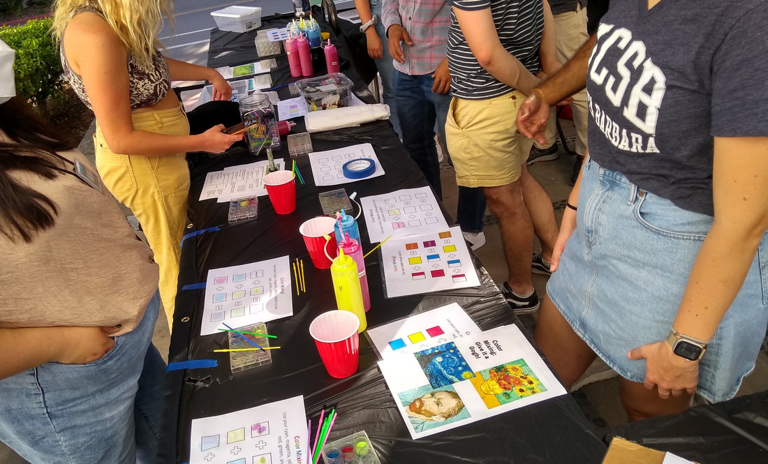
As part of the SBMA Free Community Day on April 7, 2022, the Photonics Society hosted a color mixing activity on the terrace in front of the art museum. Guests learned about additive and subtractive color mixing while having fun mixing paints. Several guests proved to be talented young artists, making beautiful recreations of Van Gogh paintings by mixing cyan, magenta, and yellow paint to create a variety of colors.
Friday March 4th at 1:00pm PST in Henley Hall 1010 and via Zoom Pizza Provided in-person! Porous semiconducting nitrides are effectively a new class of semiconducting material, with properties distinct from the monolithic nitride layers from which devices from light emitting diodes (LEDs) to high electron mobility transistors are increasingly made. The introduction of porosity provides new opportunities to engineer a range of properties including refractive index, thermal and electrical conductivity, stiffness and piezoelectricity. Quantum structures may be created within porous architectures and novel composites may be created via the infiltration of other materials into porous nitride frameworks. A key example of the application of porous nitrides in photonics is the fabrication of high reflectivity distributed Bragg reflectors (DBRs) from alternating layers of porous and non-porous GaN. These reflectors are fabricated from epitaxial structures consisting of alternating doped and undoped layers, in which only the conductive, doped layers are electrochemically etched. Conventionally, trenches are formed using a dry-etching process, penetrating through the multilayer, and the electrochemical etch then proceeds laterally from the trench sidewalls. The need for these trenches then limits the device designs and manufacturing processes within which the resulting reflectors can be used. We have developed a novel alternative etching process, which removes the requirement for the dry-etched trenches, with etching proceeding vertically from the top surface through channels formed at naturally-occurring defects in the crystal structure of GaN. This etch process leaves an undoped top surface layer almost unaltered and suitable for further epitaxy. This new defect-based etching process provides great flexibility for the creation of a variety of sub-surface porous architectures on top of which a range of devices may be grown. Whilst DBR structures enable improved light extraction from LEDs and the formation of resonant cavities for lasers and single photon sources, recent development also suggest that thick, subs-surface porous layers may enable strain relaxation to help improve the efficiency of red microLEDs for augmented reality displays. Meanwhile, the option of filling pores in nitride layers with other materials provides new opportunities for the integration of nitrides with emerging photonic materials, such as the hybrid-perovskite semiconductors, with perovskites encapsulated in porous nitride layers demonstrating greatly improved robustness against environmental degradation.

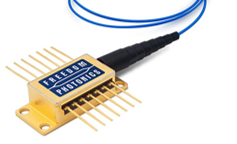
Thursday, November 18th, 11 am (PST) in Henley Hall 1010 Pizza will be provided! Cutting edge diode lasers and PICs for sensing applications Over the past several years, many new application areas for photonics in optical sensing have opened up. In this talk, we will review record performance diode laser and PIC technology developed by Freedom Photonics for a variety of optical sensing applications - gas sensing, atomic sensing and LIDAR. Basic skills for a good technical team leader Many engineers with advanced degrees end up leading high-impact technical teams, in pursuit of research, development or production. In this talk, we will discuss various practical issues related to being a good team leader.
 Join us at Henley Hall 1010 on 10/28 at 1pm! Free Pizza Provided!
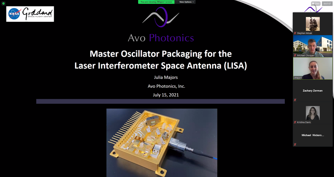
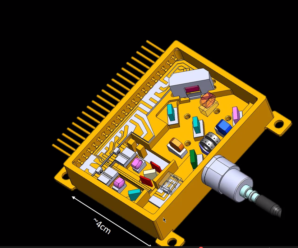
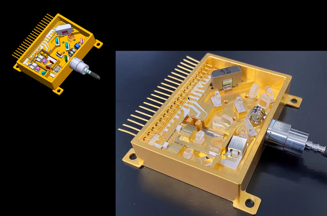
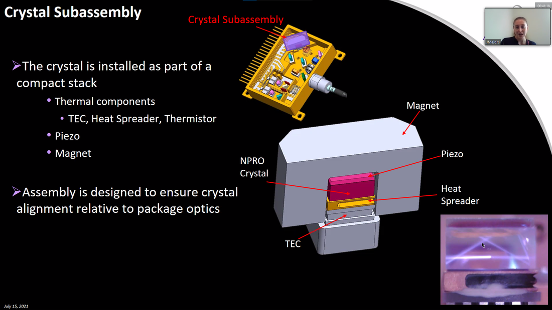
Dr. Julia Majors - Master Oscillator Packaging for the Laser Interferometer Space Antenna (LISA)7/8/2021
Thursday, July 15, 10:00 - 11:00 am (PDT) 5 years after the earth-based gravitational wave observatory, LIGO, made its first detection of gravitational waves, work is already well underway in preparing for the next generation of gravitational wave observatories – in orbit around the sun. Working with NASA Goddard Space Flight Center, we are building what will be the “quietest” oscillator in (and above) the world to serve as the core light source for the interferometric system. The system is based on a non-planar ring oscillator (NPRO) model, which I will discuss along with some of the challenges that arise when developing laser systems for space applications. Student Lecture by KaiKai Liu on Milliwatt Threshold 0.5-Hz Linewidth Si3N4 Brillouin Laser5/25/2021
Friday May 28 at 1:00 pm
 The UCSB Quantum Foundry and the UCSB Photonics Society hosted the 2021 Quantum Industry Showcase on April 22 and 23. You can watch the Keynote address and the fireside chat below. You can also find more information and presentations from the event at https://qis.quantumfoundry.ucsb.edu/. Like these videos? Watch the full QIS 2021 playlist at
https://www.youtube.com/watch?v=xulQc4G_R9w&list=PLtIKDPzlP_wMvxVLMWlnP-lP6kb7Lr29l |
Mailing ListSupported By
Thorlabs designs and produces a variety of optomechanical and optoelectronic components in 15 facilities around the globe. Thorlabs seeks to listen and serve its customers with over 20,000 products available.
Founded in 2018, Nexus Photonics has developed integrated photonics ready to scale. Smaller, lighter and faster, their platform outperforms industry benchmarks, and operates in an ultra-broadband wavelength range from ultraviolet to infrared to support a wide breadth of practical applications.

Archives
May 2024
Categories
All
|