|
|
|
|
|
|
|
|
Tuesday, Dec. 11th at 12:00 PM in Elings 3001
Pizza will be provided! 
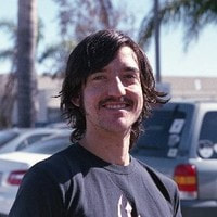
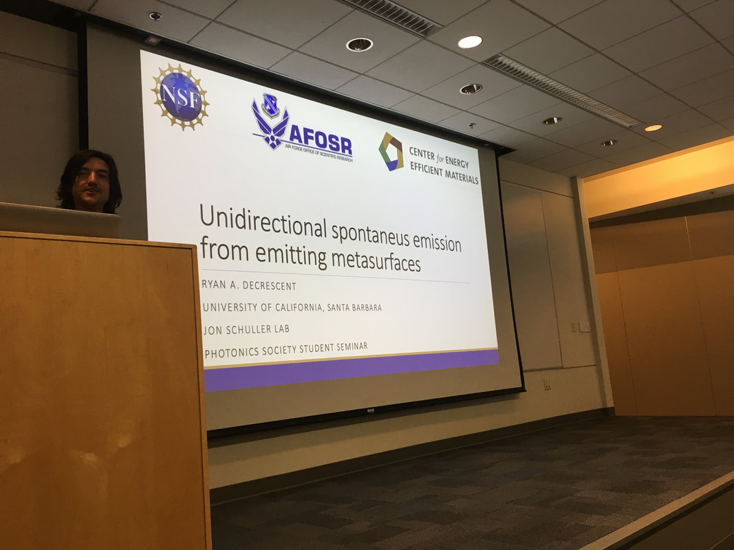
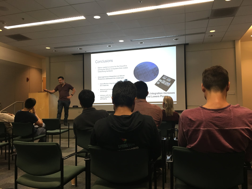
Tuesday Dec. 4th at 12:30 pm in ESB 1001 Pizza will be provided! This is the start of the weekly student lecture series IEEE Photonics is hosting throughout Winter 2019! Ryan DeCrescent and Robert Zhang will be presenting their talks.   Wednesday November 28th, 2 pm, ESB 1001 Alex is an entrepreneur with a track record of building teams that take ideas from the research laboratory through commercialization. Alex was a co-founder, the CEO, and Board Director of Aurrion from 2008-2016 which was a fabless semiconductor company that developed photonic integrated circuits for data center networking applications. The business was acquired by Juniper Networks. Alex worked for IBM, Lawrence Livermore National Laboratory, and Intel prior to founding Aurrion. Alex earned his M.S & Ph.D. from UCSB and is an alumnus of the Harvard Business School Owner/President Management Program. In his downtime, Alex enjoys riding off road motorcycles, playing guitar, smoking meat and reading books. Alex loves spending time with his wife and daughter going to live shows, travelling and eating weird stuff. Refreshments Provided!  Dr. Ken-Tye Yong Director of the Bio Devices and Signal Analysis (VALENS) School of Electrical and Electronic Engineering Nanyang Technological University (NTU) Tuesday, Nov. 20th, 3 - 4 pm, ESB 2001 Nanomaterials have been applied in healthcare applications such as cancer imaging, lymph node mapping and brain diseases therapy. These nanomaterials can be engineered to serve as a platform for challenges in highly sensitive optical diagnostic tools, biosensors, and guided imaging and therapy. The versatility of nanomaterials may provide the keys to improve diagnostics and therapy of human diseases. In this talk, we will highlight the use of nanomaterials with different sizes, compositions, and shapes for nanomedicine applications. This talk is intended to promote the awareness of past and present developments of nanomaterials in biomedical fields, the potential toxicity of nanomaterials, and the approaches to engineer new types of safe nanomaterials, whereby encouraging researchers to think about exciting and promising biophotonic and nanomedicine applications with nanomaterials in the future. Refreshments Provided!  Friday Nov 9th, 1pm, Elings 1605 The past decade has seen accelerated progress in III-V semiconductor infrared photodetector technology. The advent of the unipolar barrier infrared detector device architecture has in many instances greatly alleviated generation-recombination (G-R) and surface-leakage dark current issues that had been problematic for many III-V photodiodes. Meanwhile advances in a variety type-II superlattices (T2SLs) such as InGaAs/GaAsSb, InAs/GaSb, and InAs/InAsSb, as well as in bulk III-V material such as InGaAsSb and metamorphic InAsSb, have provided continuously adjustable detector cutoff wavelength coverage from the short wavelength infrared (SWIR) to the very long wavelength infrared (VLWIR). The confluence of these developments has led to a new generation of versatile, cost-effective, high-performance infrared detectors and focal plane arrays based on robust III-V semiconductors, providing a viable alternative to HgCdTe (MCT). Refreshments provided!  Prof.Brian Cunningham Department of Electrical and Computer Engineering, Department of Bioengineering University of Illinois at Urbana-Champaign Tuesday, Oct 16th, 11am, ESB 1001 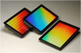 Circulating exosomal miRNA represents a potentially useful class of bloodborne biomarkers for cancer. We present the initial proof-of-concept of an approach in which gold nanoparticle tags are prepared with thermodynamically optimized nucleic acid toehold probes that displace a oligonucleotide and reveal a capture sequence that is used to selectively pull down the target-probe-nanoparticle complex to a photonic crystal (PC) biosensor surface. By matching the surface plasmon resonant wavelength of the nanoparticle tag to the resonant wavelength of the PC nanostructure, the reflected light intensity from the PC is dramatically and locally quenched by the presence of each nanoparticle. The talk described the optical operating principles of Photonic Resonator Absorption Microscopy (PRAM), the thermodynamic design of DNA toehold probes, and our first results demonstrating the detection limits, selectivity, and dynamic range of the assay. Refreshments provided! 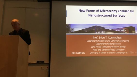 Dr. Cunningham giving his talk about Microscopy Enabled by Nanostructured Surfaces. Friday, Jun. 8th, 4:30 - 5:30 pm, ESB 2001 Communications networks and systems are seeing extreme increases in network traffic which is growing at the tremendous rate of 30% per year. It is estimated that the energy and cost requirements will increase tenfold in coming year. But this progress is not sustainable from an ecological and economic point of view. However, this information explosion can be dealt with, using the integration of very small photonic components on very high density Photonic Integrated Circuits (PICs). The technolgoical advancements in PICs have made them a popular choice for components of next generation networks. Silicon being the evident choice due to its high availability, mature fabrication technology, and low cost has attracted components on a chip. At the same time, the unique, material properties and direct bandgap of group III-V materials have huge potential in applications like laser amplifiers, modulators, and detectors. Due to robustness, flexibility, reliability, and performance of PICs, many commercial solutions are now available for a variety of applications. Refreshments Provided! 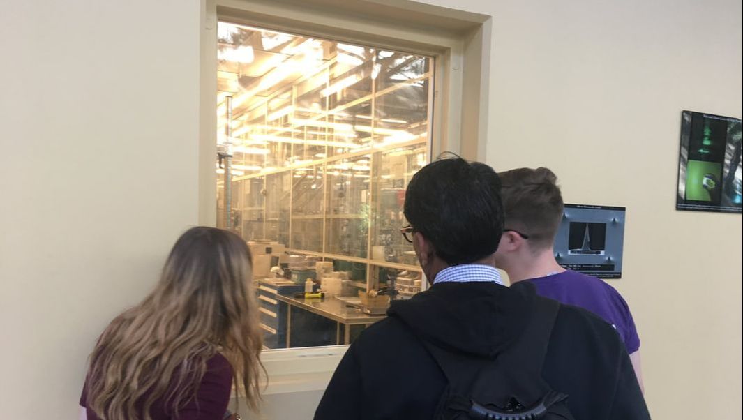 Dr. Singh looking into the UCSB nanofab cleanroom during his visit. 
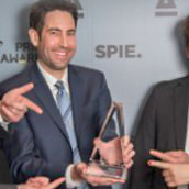
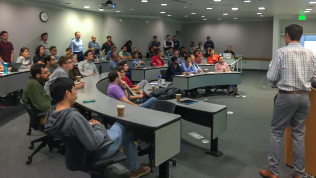
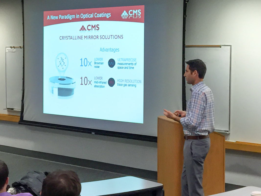
Abstract: In this presentation, Garrett provides an overview of how two scientists from the University of Vienna stumbled upon an enabling technology, born from fundamental research in the burgeoning field of cavity optomechanics, and made a successful transition from academia to industry. The fruit of this endeavor is “Crystalline Mirror Solutons,” or CMS, a photonics start-up commercializing high-performance optics for laser-based precision measurement and manufacturing systems. Here, Garrett outlines the key elements that led to their successes, including the conception of the underlying technology, as well as the supporting infrastructure and funding organizations that ultiately assisted in bringing this idea out of the laboratory and onto the commercial market. Bio: Dr. Garrett D. Cole, Co-Founder of Crystalline Mirror Solutions (www.crystallinemirrors.com), obtained his PhD in Materials from the University of California, Santa Barbara in 2005. Since completing his doctorate, he has held positions ranging from the first employee of a high-tech startup (Aerius Photonics LLC, now FLIR Electro-Optical Components), to a postdoctoral position at Lawrence Livermore National Laboratory, a Marie Curie Fellow of the Austrian Academy of Sciences, and, prior to leaving to found CMS, an assistant professor in the Faculty of Physics at the University of Vienna. In the course of his research career, Dr. Cole has co-authored 2 book chapters and published more than 50 journal articles and conference proceedings including papers in Science, Nature, Physical Review Letters, and the Proceedings of the National Academy of Sciences. Leveraging his expertise in micro- and nanofabrication, tunable lasers, and cavity optomechanics, Dr. Cole developed the proprietary substrate-transfer process at the heart of Crystalline Mirror Solutions and, along with Professor Markus Aspelmeyer, co-founded the venture in February 2012.
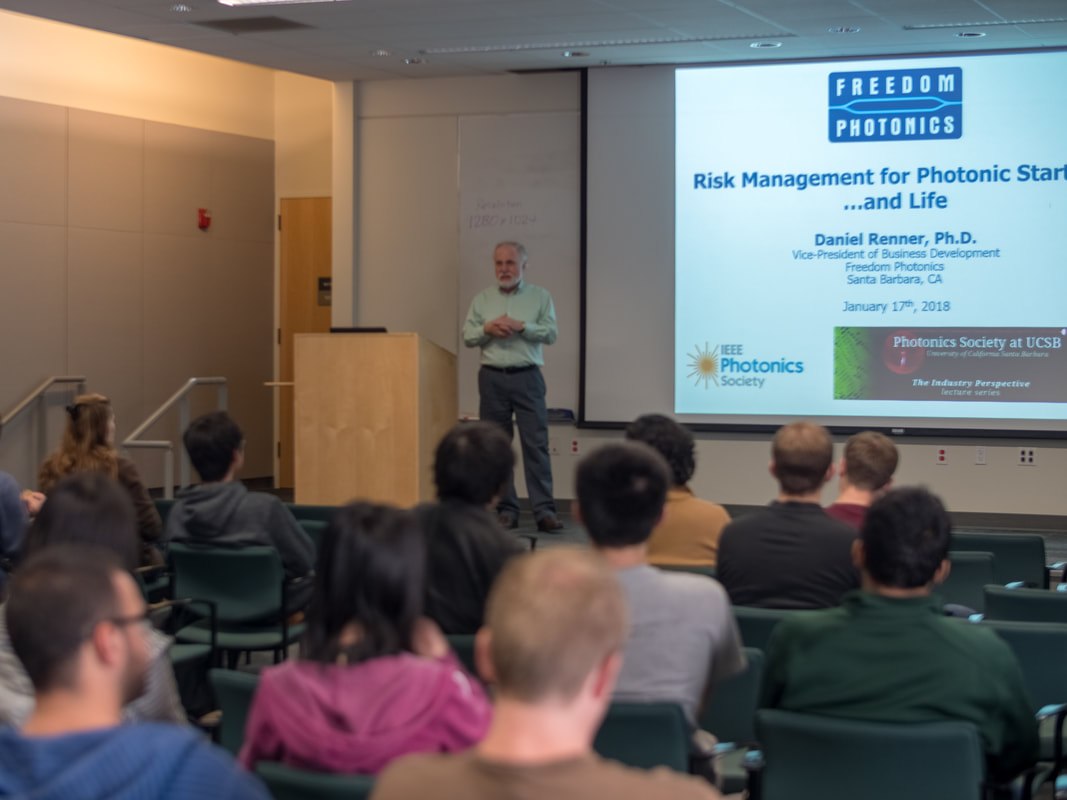
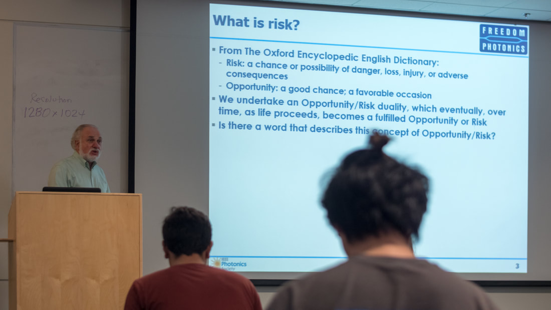
Abstract: Success in a photonic startup company requires constant attention to the balance between risk and opportunity. These risk / opportunity decisions involve many different areas, technical, marketing, financial, organizational and psychological, among others. Some of these decisions are very specific to photonic startup issues but the balance of opportunity and risk touches on a broad range of aspects of life, of course. This presentation discussed the general nature of risk and opportunity and from these general ideas will then derive recommendations for effective risk management methods in photonic startups. The presenter did this through examples drawn from his own experience and from the experience of others that have influenced him strongly Bio: Dr. Daniel Renner received a Ph.D in Opto-Electronics from the University of Cambridge in England. This has been followed by 37 years of industrial experience, where he has been deeply involved with the development, manufacturing and commercialization of complex photonic devices and systems used in communication, sensor and industrial applications. His experience spans both the technical and the commercialization aspects of photonic products, having led activities in many areas, including technology and product development, identification of new business areas, introduction of new products, marketing and sales. Through this experience he has gained a respectful appreciation for the critical importance of effective business risk management. 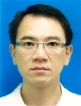 Where: ESB 1001
When: Friday, June 9, 12:00PM Lunch will be provided Abstract: The excitement of nanowire research is due to the unique electronic and optical properties of these nanostructures. Both axial and radial heterostructure nanowires have been proposed as nano‐building blocks for the next generation devices, which are expected to revolutionise our technological world. The unique properties stem from their large surface area‐to‐volume ratio, very high aspect ratio, and carrier and photon confinement in two dimensions. These nanowires are usually grown by the so‐called vapor‐liquid‐solid mechanism, which relies on a metal nanoparticle to catalyze and seed the growth. An alternative technique to grow the nanowires is by selective area growth technique, where a dielectric mask is first patterned on the substrate prior to growth. In this talk, I will present an overview of compound semiconductor nanowire research activities at The Australian National University. The optical and structural properties of binary and ternary III‐V nanowires including GaAs, InGaAs, InP and GaAsSb nanowires grown by metal‐ organic vapour phase epitaxy will be presented. Various issues such as tapering of the nanowires, compositional non‐uniformity along nanowires, crystal structure, carrier lifetime and polarization effect will be discussed. I will also present our results of III‐V nanowires grown on Si substrates which are of great interests for the integration of nano‐optoelectronic devices on Si platforms. Our results of enhancing the quantum efficiency of nanowires by using plasmonics are promising to improve the performance of nanowire devices. Finally, the results from our nanowire lasers, photodetectors, solar cells and photoelectrodes for water splittng will be presented. Bio: Professor H. Hoe Tan is currently the Head of the Department of Electronic Materials Engineering at the Research School of Physics and Engineering, The Australian National University. He received his B.E. (Hons) in Electrical Engineering from the University of Melbourne in 1992, after which he worked with Osram in Malaysia as a quality assurance engineer. In 1997, he was awarded the PhD degree from the Australian National University for his dissertation on "Ion beam effects in GaAs‐AlGaAs materials and devices". He has been the past recipient of the Australian Research Council Postdoctoral, QEII and Future Fellowships. He has published/co‐published over 350 journal papers, including four book chapters. He is also a co‐inventor in 4 US patents related to laser diodes and infrared photodetectors. His research interests include epitaxial growth of lowdimensional compound semiconductors, nanostructured optoelectronic devices and ion‐ implantation processing of compound semiconductors for optoelectronic device applications. Prof. Tan is a Senior Member of the IEEE.
Date: Wednesday, May 10, 2017
Location: UCSB, Engineering Science Building, Rooms ESB1001, ESB 2001, ESB 2003
Join us for our spring event the 2017 Light Science Workshop for a day of talks and presentations about the cutting edge in photonics research and career opportunities in this blossoming industry. The event will feature a keynote speaker, technical and non-technical presentations, Q&A panels, a job fair and a poster session!
The presentations will have two tracks: Technical and non-technical. The Technical Track will feature lectures on cutting-edge research in the area from varying fields that use and manipulate light. The Non-Technical Track will focus on careers in the industry and professional development. Keep checking back on this page for the most up-to-date information! The event is free for those affiliated with a university or college. Otherwise, general admission to the event is $20.
If you are interested in sponsoring the event or holding a booth at the career fair, please contact us
Agenda
Please see our Program of Events for more information!
Keynote Speech — Seeing Heat: Thermal Vision Everywhere You Look
Technical and Non-technical Presenters
Technical and Non-technical talks will include presentations from speakers representing research groups, photonics companies, and partnerships and collaborations at UCSB and around Santa Barbara. A sample of our scheduled speakers will include the following:
Optoelectronics Research Group of John Bowers Dan Blumenthal, Optical Communication and Photonic Integration Group Phil Lubin, UCSB Experimental Cosmology Group AIM Photonics Freedom Photonics Unite To Light Center for Science and Engineering Partnerships (CSEP) at CNSi UCSB Nanofabrication Facility Event Flyer
This event is made possible with the generous support of:

 2nd Annual Photonics Society Banquet When: Wednesday May 4th, 6pm Where: Mosher Alumni House at UCSB Presented in collaboration with AIM Photonics! Graduate Students: FREE Non-Students: $15 Dinner & Drinks included (21+ Only) The 2016 banquet was hosted in collaboration with the American Institute of Manufacturing: Photonics. Dean of the College of Engineering Rod Alferness talked about UCSB being the west coast hub for National Photonics Manufacturing Institute Here are a few pictures for the imaginative photonics community at Santa Barbara: See our 2014 Banquet here. Joshua Smith From Cal State Fullerton delivered a fantastic keynote lecture on the recent detection of Gravitational Waves at LIGO. Keynote Lecture
 Simulation of a binary black-hole system. Simulation of a binary black-hole system. On September 14, 2015 the two detectors of the Laser Interferometer Gravitational Wave Observatory (LIGO) detected gravitational waves from the coalescence of a binary system of black holes. This discovery could not have been made without a century of advances in optical technology and precision metrology. I will give an overview of gravitational waves and LIGO, describe the optics involved and current optical challenges, discuss the discovery of gravitational waves from a merging binary black hole system, and end with prospects for future gravitational- wave observations.  Joshua Smith directs the Gravitational-Wave Physics and Astronomy Center (GWPAC) and is an associate professor of physics at California State University, Fullerton. He was born in Indian Lake, NY and attended Syracuse University, graduating with a BSc in 2002. He earned his doctorate in 2006 from the University of Hannover's Max Planck Institute for Gravitational Physics / Albert Einstein Institute for his work on the GEO600 gravitational-wave detector. Prior to joining Fullerton in 2010, he was a postdoctoral research associate at Syracuse University. Currently, Smith is active in gravitational research, astronomy education research, and teaching physics and astronomy. His research is focused on detecting gravitational waves from astronomical sources using LIGO in collaboration with colleagues in GWPAC and in the international LIGO Scientific Collaboration. Additionally, look forward to talks by our sponsors:
Agenda: Social Time & Dinner: Appetizers & Drinks (one complimentary drink is included with ticket) Keynote: Joshua Smith: Using optics and precision metrology in LIGO to measure black hole mergers from across the universe AIM-Photonics: Dean of Engineering Rod Alferness Talks from Sponsors: Hewlett Packard Labs, Freedom Photonics The Balcony & Library will be set aside for Networking/Socializing.
Who: Dr. Ardavan Oskooi, Founder and CEO of Simpetus When: Thursday, October 29th 12:00 pm Where: ESB 2001 Snacks & Coffee will be provided. UPDATED: Ardavan Osooki is offering to meet personally with interested students and researchers to discuss how to use his electromagnetics FDTD software for your specific simulations, or how to how to program an FDTD software from scratch, as he has done. If you are interested in a one-on-one meeting with him, please email to Tanya Das tdas@ece.ucsb.edu with your availability on Thursday, October 29th, and we will get back to you with a meeting time.   Abstract: Advances in computational electrodynamics have the potential to enable fundamentally new kinds of designs in nanophotonic devices which are based principally on complex, non-analytical wave-interference effects. Powerful, flexible, open-source software tools have now been made available for use in large-scale, parallel computations to model the interaction of light with practically any kind of material in any arbitrary geometry. These recent developments in computational capability make possible the investigation of various emergent structures and physical phenomena that were previously beyond the reach of pencil-and-paper analytical methods as well as less versatile and even less accessible commercial software tools. Here, I demonstrate how such advances in finite-difference time-domain (FDTD) methods for computational electromagnetism via an open-source software package known as MEEP can lead to entirely new designs for light trapping in nanostructured thin-film silicon solar cells as well as light extraction from nanostructured organic light-emitting diodes (OLEDs). In the last part of this seminar, I will provide a live demonstration of launching MEEP simulations on an on-demand high-performance computing (HPC) cluster in the cloud through our startup, Simpetus. Simpetus provides a holistic solution to the three main challenges of using simulations for research and development: 1) no software licenses or installation, 2) no hardware acquisition or maintenance and 3) technial support from the experts. The mission of Simpetus is to propel computational simulations to the forefront of photonics research and development.
Bio: Ardavan Oskooi is the Founder and CEO of Simpetus, a San Francisco- startup offering an on-demand photonics simulation platform with a mission to propel computational simulations to the forefront of photonics R&D. Ardavan received his Sc.D. from MIT where he worked with Prof. Steven Johnson and John Joannopoulos (thesis: Computation & Design for Nanophotonics) to develop MEEP (ab-initio.mit.edu/meep). Ardavan has published 13 first-author articles in peer-reviewed journals and a book "Advances in FDTD Computational Electrodynamics: Photonics and Nanotechnology” with Prof. Allen Taflove of Northwestern University and Steven Johnson. He has a masters in Computation for Design and Optimization from MIT and completed his undergraduate studies, with honors, in Engineering Science at the University of Toronto. Prior to launching Simpetus, he worked with Prof. Susumu Noda at Kyoto University and Stephen Forrest at the University of Michigan on leveraging MEEP to push the frontier of optoelectronic device design Who: Prof. Amnon Yariv, Dept. of Applied Physics and Electrical Engineering at CalTech When: Friday Jan. 23rd, 4:00 pm Where: Eng. Sciences Building 2001 Snacks & Coffee will be provided  Abstract: The talk will describe the theory, design, fabrication, and the experimental results of an effort that led to a new type of hybrid Si/III-V semiconductor (SCL) laser with a linewidth below 1 KHz. This result is nearly 3 orders of magnitude better (smaller linewidth) than that of commercial SC lasers. Other key parameters relevant to coherence such as the phase/amplitude coupling constant, α, and the relaxation resonance frequency are reduced by more than an order of magnitude. The fabrication employed is CMOS compatible making the new laser integrable with electronic circuits and potentially enabling a new generation of communication, time-keeping, and sensing applications.  Bio: Amnon Yariv is the Martin and Eileen Summerfield Professor of Applied Physics and Electrical Engineering at Caltech. He obtained the B.S. (1954), M.S. (1956) and Ph.D. (1958) in electrical engineering from the University of California at Berkeley. He went to the Bell Telephone Laboratories, Murray Hill, New Jersey in 1959, joining the early stages of the laser effort. He came to the California Institute of Technology in 1964.
On the technical side, he is responsible with W. H.Louisell and A.E. Siegman for the quantum mechanical formulation of parametric (nonlinear) optics. With students and various colleagues, he proposed and demonstrated the fields of: Optoelectronic Integrated Circuits (IOECS), the Distributed Feedback Semiconductor laser, and coupled-resonator optical waveguide. His recent research is on 3D lidar imaging with swept frequency semiconductor lasers and limits of coherence of semiconductor lasers. Dr. Yariv is a member of the American Physical Society, Phi Beta Kappa, the American Academy of Arts and Sciences, the National Academy of Engineering, the National Academy of Sciences, a Fellow of the Institute of Electrical and Electronics Engineers and the Optical Society of America. He was the recipient of the 1980 Quantum Electronics Award of the IEEE, the 1985 University of Pennsylvania Pender Award, the 1986 Optical Society of America Ives Medal, the 1992 Harvey Prize, the 1998 OSA Beller Medal, the National Medal of Science 2010, and the IEEE Photonics Award 2011. Dr. Yariv was a founder and chairman-of-the-board of ORTEL Corporation (acquired by Lucent Technologies in 1998), and is a founder and a board member of a number of startup companies in the optical communications field. Who: Prof. Joyce Poon, University of Toronto, Dept. of Electrical Engineering When: Thursday October 9th, 4:00 pm Where: Eng. Sciences Building (ESB), Room 2001
Abstract: The surging progress in silicon photonics over the past decade has been driven by its potential application in low cost, high bandwidth, wavelength-division multiplexed short reach optical interconnect. Despite significant advances, numerous technical challenges remain, such as the control of resonant devices, the implementation of large swing optical modulators, the management of polarization, the need for improved variation tolerance, an effective means for efficient and broadband fiber-to-chip optical coupling, and approaches to electronic-photonic integration. In this talk, I will provide an overview of my group’s progress in addressing these issues in silicon-based photonic platforms. Photonic devices and integrated circuits implemented in standard silicon-on-insulator photonic platforms and a custom silicon nitride-on-silicon platform will be presented. I will describe microring modulators and filters that circumvent conventional limits, the first polarization rotator-splitters and controllers in standard silicon photonic platforms, grating couplers with record-setting bandwidths and insertion losses, and our ongoing efforts in electronic integration. The work paves the path toward very large- scale photonic integrated circuits and terabit-scale optical transceivers.  Bio: Joyce Poon is an Associate Professor of Electrical and Computer Engineering at University of Toronto, where she holds the Canada Research Chair in Integrated Photonic Devices. She is currently a Visiting Associate in Electrical Engineering at Caltech. She and her team conduct theoretical and experimental research in micro- and nano-scale integrated photonics
Dr. Poon obtained her Ph.D. and M.S. in Electrical Engineering from Caltech in 2007 and 2003 respectively, and the B.A.Sc. in Engineering Science (physics option) from the University of Toronto in 2002. She is the recipient of a McCharles Prize for Early Research Career Distinction, a MIT TR35 award in 2012, IBM Faculty Award in 2010 and 2011, Ontario Ministry of Research and Innovation Early Researcher Award in 2009, NSERC University Faculty Award in 2008, and the Clauser Doctoral Thesis Prize from Caltech in 2007.
Abstract: Today’s fiber-optic communication networks span the globe, delivering broadband information across all market segments and connecting massive datacenters, businesses, and individual user’s homes. As such, optical networks must operate reliably and efficiently when transporting the massive information capacity of the Internet, allowing networks to adapt to growing and changing demand flows and occasional interruptions. Wavelength-selective switches (WSS) have been instrumental in fulfilling this role, enabling all-optical spectral routing of individual wavelength-division multiplexed (WDM) communication channels at network nodes. The recent introduction of space-division multiplexing (SDM) to the optical communication domain with new fiber types, in order to economically support the exponentially growing capacity, necessitates complementary components for implementing SDM-WDM optical networks. SDM is typically realized with either multi-core or few-mode fibers and great capacity achievements have been demonstrated to-date in each fiber solution. Wavelength-selective switching functionality for these two fiber types has recently been introduced. A joint- switching WSS concept has been realized for multi-core fibers, enabling information to be encoded and routed on the SDM-WDM optical network as a spatial super-channel (single wavelength channel spanning multiple cores). This spatial super-channel routing concept with joint-switching WSS also extends to few- mode fibers. Hence a single WSS can then be used in analogous fashion to the single-mode fiber networks, thereby heralding the cost-savings benefits of SDM. A WSS with direct few-mode fiber interfaces has been demonstrated with the few-mode beams routed in free-space just as the single mode beam does in a conventional WSS. A study on the pass band filtering effect and mode mixing due to the spectral switching of dispersed components revealed the spatial-spectral interplay in the mode-dependent loss attributes of the few- mode fiber WSS. Such advanced WSS prototypes will serve the next generation transport networks when SDM is fully adopted by carriers.  Bio: Prof. Dan Marom joined the faculty of the Applied Physics Department in the fall of 2005, where he is pursuing his research interests in creating photonic devices for switching and manipulating optical signals. Dan earned the B.Sc. degree in Mechanical Engineering in 1989, and the M.Sc. degree in Electrical Engineering in 1995, both from Tel-Aviv University's School of Engineering. He was awarded the Ph.D. degree in Electrical Engineering by the University of California, San Diego , in 2000. From 2000 until 2005, Dan was employed as a Member of the Technical Staff at Bell Laboratories , then part of Lucent Technologies.
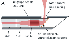 Abstract: Microscopy is usually performed in a laboratory on carefully prepared, very thin samples and achieves resolutions of better than a micrometer. Medical imaging, by contrast, is usually performed on sizeable portions of the living human body, and resolutions are rarely better than 1 millimeter. Over the last decade, there has been great progress in applying optical microscopy techniques to the human body in a medical setting. This push has been led by optical coherence tomography (OCT), which is now in mainstream use in ophthalmology and is gaining acceptance in cardiology. In this talk, 3D microscopic imaging deep inside tissue using the OCT microscope in a needle will be described. Needle delivery makes optical imaging possible in many tissues previously inaccessible to optics. Aimed to be broadly accessible, this talk will describe the underpinning photonics and guided-wave optics design and fabrication needed to make high-quality micro-imaging possible. Technical advances such as realization of ultra-small needle probes, extended imaging depth of focus, handheld micrometer-resolution tracking, and multimodality needle probes combining OCT with fluorescence, and with elastography will be presented. It will describe how such probes are built into photonic systems and where they are being applied, such as in breast cancer surgery, as well as how the technology may evolve and where it may be applied in the future.  Bio: Winthrop Professor Sampson is Director of the Centre for Microscopy, Characterization & Analysis, a core facility of the University of Western Australia, and heads the Optical + Biomedical Engineering Laboratory (OBEL) in the School of Electrical, Electronic & Computer Engineering. He directs the Western Australian nodes of the Australian Microscopy & Microanalysis Research Facility and Australia’s National Imaging Facility. He is a Fellow of the OSA and the SPIE, and an Associate Editor of IEEE Photonics Journal, the IEEE Transactions of Biomedical Engineering and on the editorial boards of the Journal of Biomedical Optics and the journals Photonic Sensors and Photonics & Lasers in Medicine. W/Prof. Sampson’s research interests are in biomedical optical engineering, with an emphasis on photonics, imaging and microscopy. His current main interest, beyond advancing microscope-in-a-needle technology, is in optical elastography – the imaging of tissue mechanical properties. His other interests include anatomical optical coherence tomography for imaging in human airways, and holographic microscopy.  Dr. Sampson & IPS President Sudha Srinivasan. 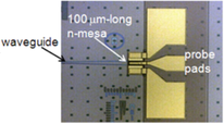  Summary: Photodetectors continue to play a crucial role in fiber optic communication systems and microwave photonics as applications demand higher bandwidths, larger power levels, and increased spectral efficiencies. High-speed, high-power photodetectors are needed as conventional top-illuminated p-i-n photodiodes cannot achieve the requisite bandwidth-efficiency products, while output power levels cause a move to side-illuminated waveguide photodiodes, photodiode arrays, and novel epitaxial layer structures. Furthermore, photodetectors incorporated into photonic integrated circuits enable more complex receiver architectures for the detection of advanced modulation formats guaranteeing the highest performance and packing density at the lowest cost.
In my talk, I provide a brief introduction to photodiode fundamentals, considerations of material systems and basic structures. I present state-of-the-art 145 GHz-waveguide photodiodes and high-power photodetector arrays that have been successfully operated at bitrates as high as 160 Gbit/s and discuss the development of an integrated dual-polarization coherent receiver that has become a key component in today’s 100 Gbit/s and emerging 400 Gbit/s fiber optic links. I cover novel device structures and photodiode arrays that enabled photonic generation of highly linear microwave signals at record-high output power levels. This includes heterogeneously integrated InP-based photodiodes on silicon that achieved the highest saturation current-bandwidth products on a silicon photonics platform to date. Bio: Dr. Andreas Beling received the Dipl.-Phys. degree (M.S.) in physics from the University of Bonn, Germany, in 2000 and the Dr.-Ing. degree (Ph.D.) in electrical engineering from Technical University Berlin, Germany, in 2006. He was a staff scientist in the photonics division at the Heinrich-Hertz-Institut in Berlin in 2001-2006, a Research Associate in the Department of Electrical and Computer Engineering at the University of Virginia in 2006-2008, and has two years of industry experience as a project manager working on optoelectronic receivers for high-speed fiber optic communication systems. He returned to University of Virginia in late 2010 as a Research Scientist and became Assistant Professor in the Department of Electrical and Computer Engineering at U.Va in 2013. His research interests include high-speed photodiodes, photonic integration technologies, and optoelectronic receivers for digital communications. Andreas Beling has authored or co-authored more than 100 technical papers, two book chapters, and three patents. He is a member of the IEEE Photonics Society and the Optical Society of America. Confessions of a Serial Entrepreneur: 30 Years of Photonic Start-ups in Academia and Industry9/16/2013
Summary: Every company – even the largest household names such as Google or Apple or even IBM - begins life as a start-up. Drawing on experience gained from Dr. Poole’s extensive start-up history, this presentation will look at how some of the companies and research groups in which Dr. Poole has been involved got started, what they did and how they subsequently developed and thrived. The presentation aims to inspire researchers who are considering how to commercialize their research to take the next steps and move out of the research lab and into the brave new world of commercialization. Dr. Simon Poole is an engineer/entrepreneur with over 30 years experience in photonics in research, academia and industry. He has been involved in numerous successful start-ups in both Academia and industry and is renowned for both his contribution to the technology of photonics as well as the companies he has founded. 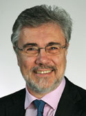 Bio: Dr. Simon Poole is an engineer/entrepreneur with over 30 years experience in photonics in research, academia and industry. He obtained his PhD from Southampton University in 1987 and was a member of the team that invented the Erbium-Doped Fiber Amplifier (EDFA) in 1985. In 1988 he moved to Australia and founded the Optical Fiber Technology Centre (OFTC) and subsequently Australian Photonics Cooperative Research Centre (APCRC) at the University of Sydney where he was director of the Sydney Node from 1991 to 1995. The APCRC grew to over 150 researchers and led to 15 start-ups which raised a total of over $250m in Venture Capital funding. In 1995, Dr. Poole led the first spin-off company from the APCRC, Indx Pty Ltd which manufactured Fiber Bragg Gratings (FBGs) for optical communications. Indx was acquired by Uniphase Corporation (now JDS Uniphase) for $US6m and subsequently grew to over 300 people with exports of over $100m pa. After leaving JDSUniphase in late 2000 he worked as a venture partner with KPLJ Ventures before co-founding Engana Pty Ltd in September 2001. As Engana’s CEO Dr. Poole raised $13m in VC funding and oversaw the development and launch of Engana’s market-leading Dynamic Wavelength Processor line of Wavelength Selective Switches in early 2005. The company, now Finisar Australia, employs 280 people in Sydney and a similar number in China, with annual sales of Wavelength Selective Switches of >$100m pa. In 2008, Dr. Poole started a new group within Finisar, the New Business Ventures Group, to generate new, high value added businesses using the principles of Open Innovation. The first business within this group was the highly successful WaveShaper range of Programmable Optical Processors which already has sales of over $6m pa. Dr. Poole is a Fellow of the IEEE in 2001 and is also a Fellow of the Institute of Engineers Australia (FIEAust), a Senior Member of the Institute of Engineering and Technology (SMIET) and a Chartered Engineer (CEng). He has published over 150 refereed papers in journals and international conferences as well as filing 7 patents, including the initial patent on the EDFA. 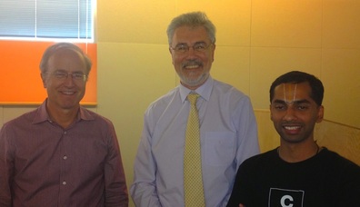 Prof. John Bowers, Dr. Simon Poole & IPS President Sudha Srinivasan after Dr. Poole's lecture. Dr. Simon Poole gave a fantastic lecture, attended by researchers from many fields beyond photonics. 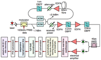
Summary: With the remorseless growth in demand for telecommunication services, the capacity of optical fiber links first exceeded the capabilities of electronics, requiring the introduction of wavelength division multiplexing, and is now approaching a fundamental limit. This limit is due to a trade-off between the familiar Shannon limit at low signal powers, and nonlinear effects at high powers. Before considering the implications of the capacity crunch when demand finally hits this limit, this lecture will review the technological achievements which took the industry from its first commercial service with the Dorset (UK) police in 1975 through to the 10 Tbit/s systems of today. 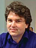 Bio:
Dr. Andrew Ellis was born in Underwood, England in 1965 and gained a BSc in Physics with a minor in mathematics from the University of Sussex, Brighton, England in 1987. He was awarded his PhD in Electronic and Electrical Engineering from The University of Aston in Birmingham, Birmingham, England in 1997 for his study on All Optical Networking beyond 10 Gbit/s. He previously worked for British Telecom Research Laboratories as a Senior Research Engineer investigating the use of optical amplifiers and advanced modulation formats in optical networks and the Corning Research Centre as a Senior Research Fellow where he led activities in high speed optical component characterization. Currently, he heads the Transmission and Sensors Group at the Tyndall National Institute in Cork, Ireland, where he is also a member of the Department of Physics, University College Cork. He is also an adjunct Professor of Electronic Engineering at Dublin City University, and a founder of the Dublin based start-up Pilot Photonics. He research interests include all optical OFDM, optical and electrical signal processing, the mechanisms limiting capacity in optical communication systems, and the application of photonics to sensing. Dr. Ellis is a member of the Institute of Physics and the Institute of Engineering Technology, and is a Chartered Physicist. He is an Associate Editor of Optics Express and acts as a reviewer for IEEE Journal of Lightwave Technology, Photonics Technology Letters and Journal of Selected Topics in Quantum Electronics. He has published over 150 journal papers and over 24 patents in the field of Photonics. |
Mailing ListSupported By
Thorlabs designs and produces a variety of optomechanical and optoelectronic components in 15 facilities around the globe. Thorlabs seeks to listen and serve its customers with over 20,000 products available.

Founded in 2018, Nexus Photonics has developed integrated photonics ready to scale. Smaller, lighter and faster, their platform outperforms industry benchmarks, and operates in an ultra-broadband wavelength range from ultraviolet to infrared to support a wide breadth of practical applications.

Archives
April 2024
Categories
All
|
||||||||||||||||||||||||||||||||||||||||||||||||||||||||||