|
|
|
|
|
|
|
|
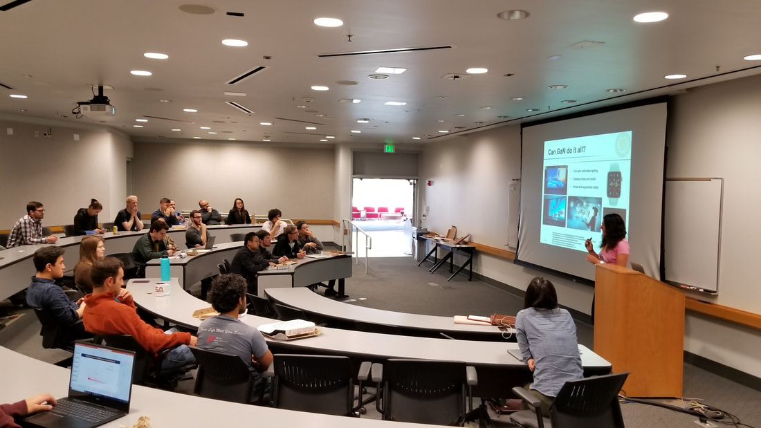
 Join us at Henley Hall 1010 on 10/28 at 1pm! Free Pizza Provided!
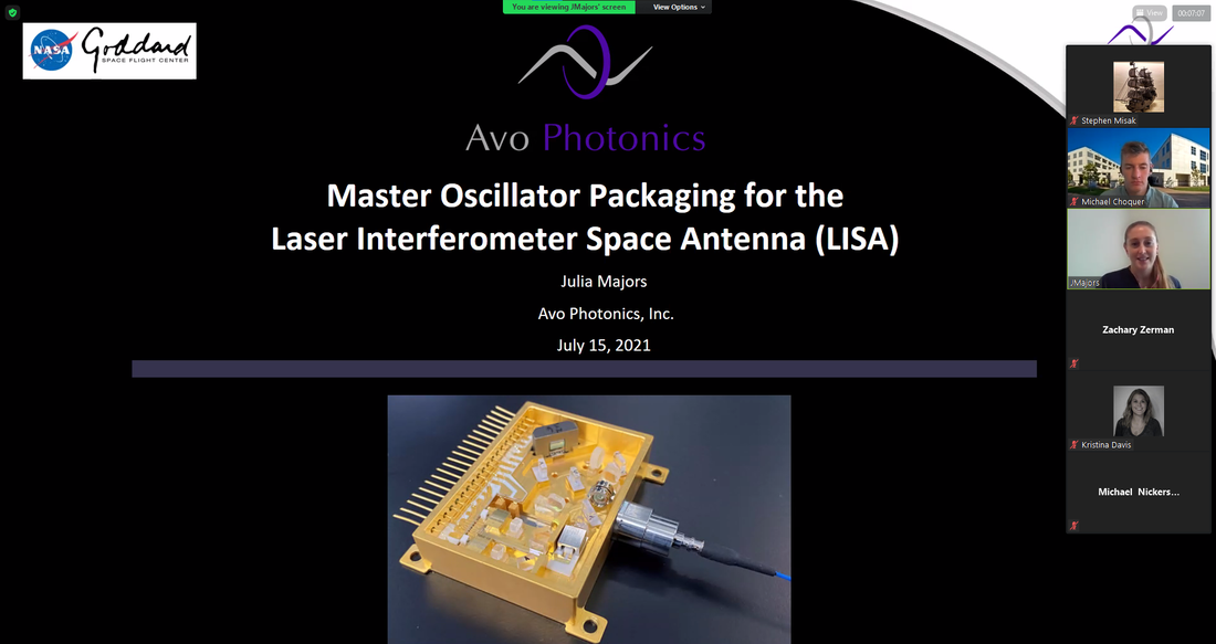
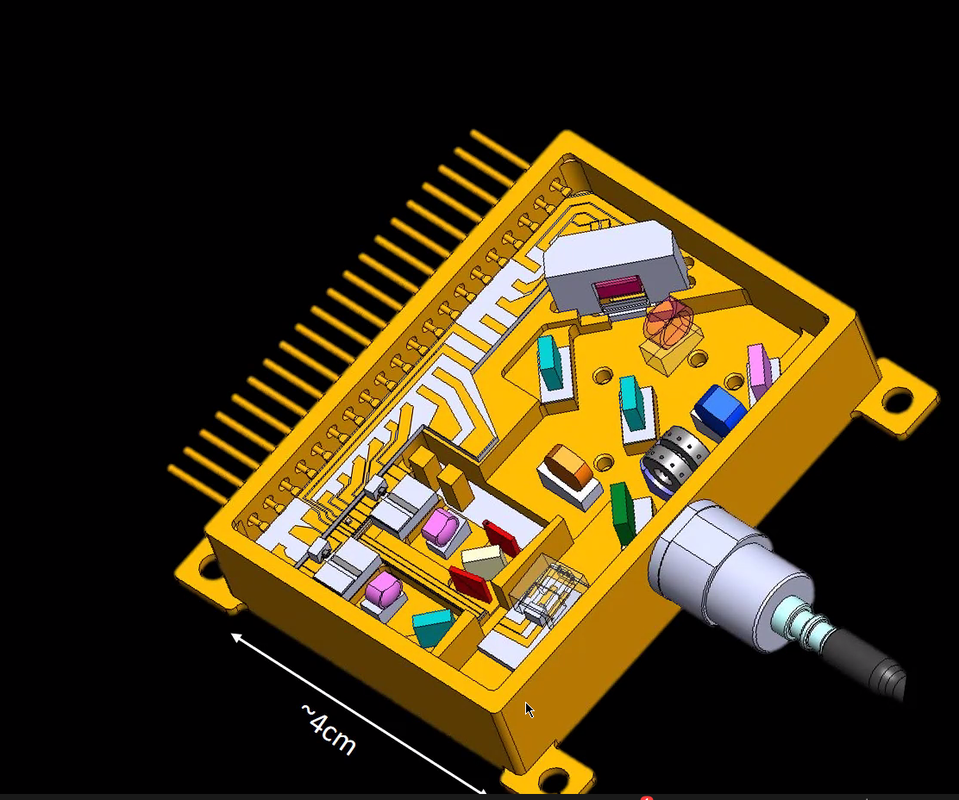
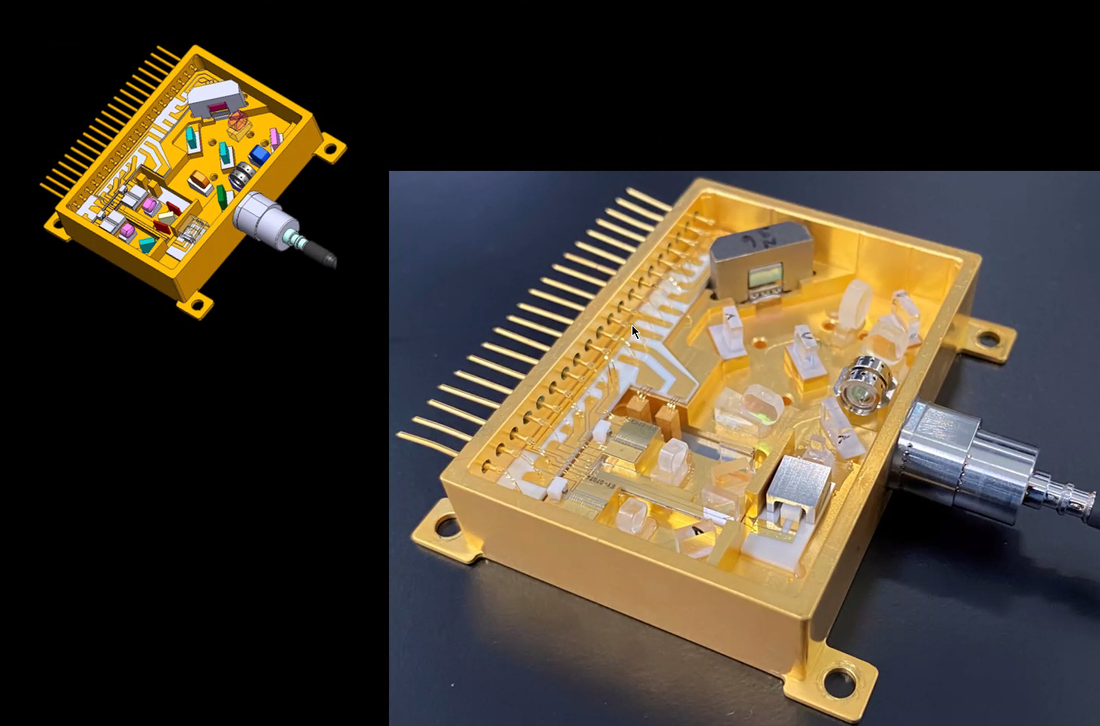
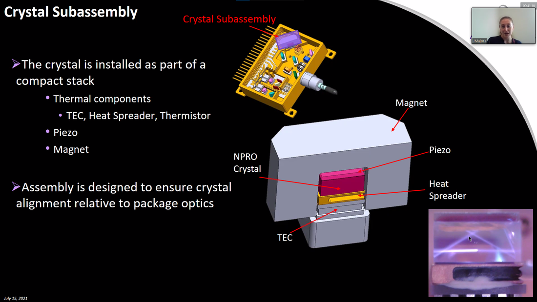
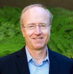
Dr. Julia Majors - Master Oscillator Packaging for the Laser Interferometer Space Antenna (LISA)7/8/2021
Thursday, July 15, 10:00 - 11:00 am (PDT) 5 years after the earth-based gravitational wave observatory, LIGO, made its first detection of gravitational waves, work is already well underway in preparing for the next generation of gravitational wave observatories – in orbit around the sun. Working with NASA Goddard Space Flight Center, we are building what will be the “quietest” oscillator in (and above) the world to serve as the core light source for the interferometric system. The system is based on a non-planar ring oscillator (NPRO) model, which I will discuss along with some of the challenges that arise when developing laser systems for space applications. Student Lecture by KaiKai Liu on Milliwatt Threshold 0.5-Hz Linewidth Si3N4 Brillouin Laser5/25/2021
Friday May 28 at 1:00 pm
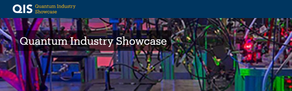 The UCSB Quantum Foundry and the UCSB Photonics Society hosted the 2021 Quantum Industry Showcase on April 22 and 23. You can watch the Keynote address and the fireside chat below. You can also find more information and presentations from the event at https://qis.quantumfoundry.ucsb.edu/. Like these videos? Watch the full QIS 2021 playlist at
https://www.youtube.com/watch?v=xulQc4G_R9w&list=PLtIKDPzlP_wMvxVLMWlnP-lP6kb7Lr29l  1:00 PM Friday, April 2nd
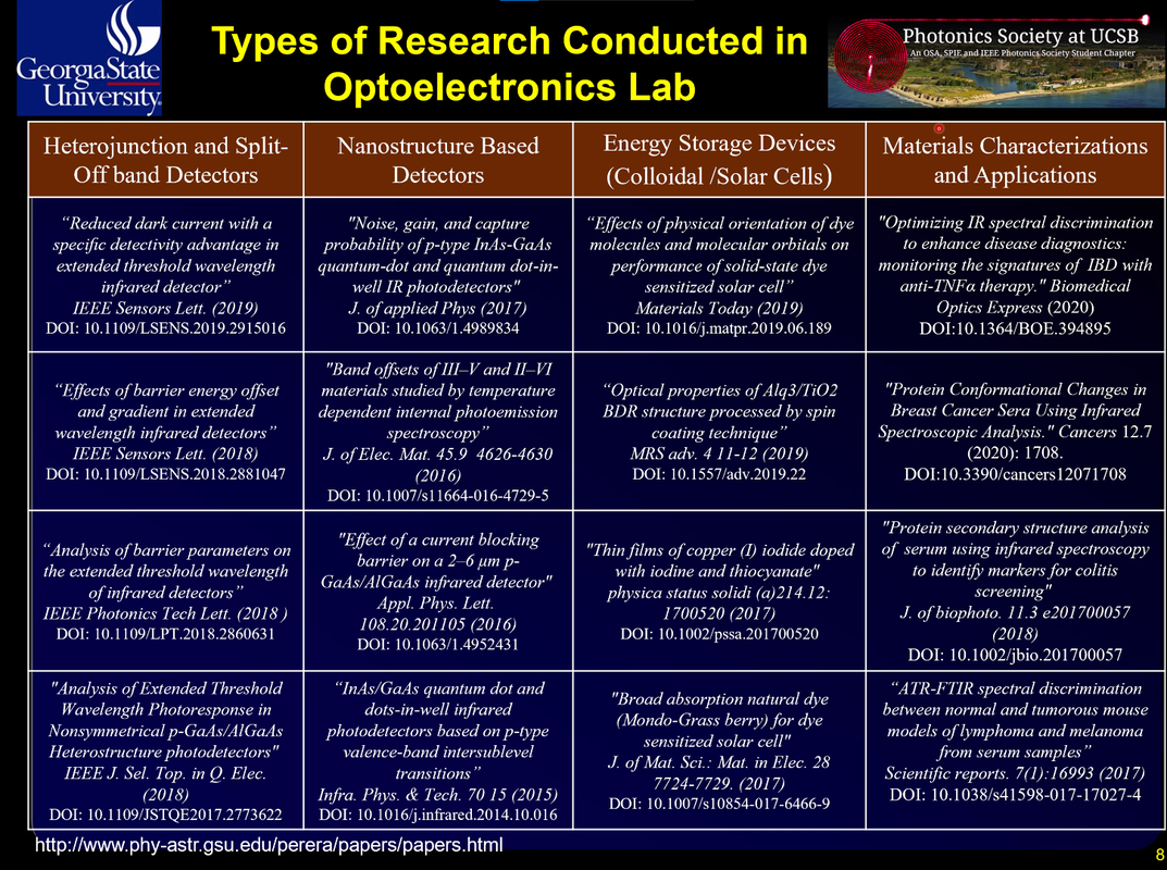
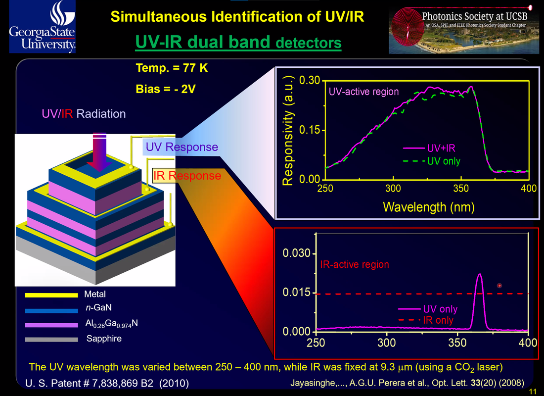
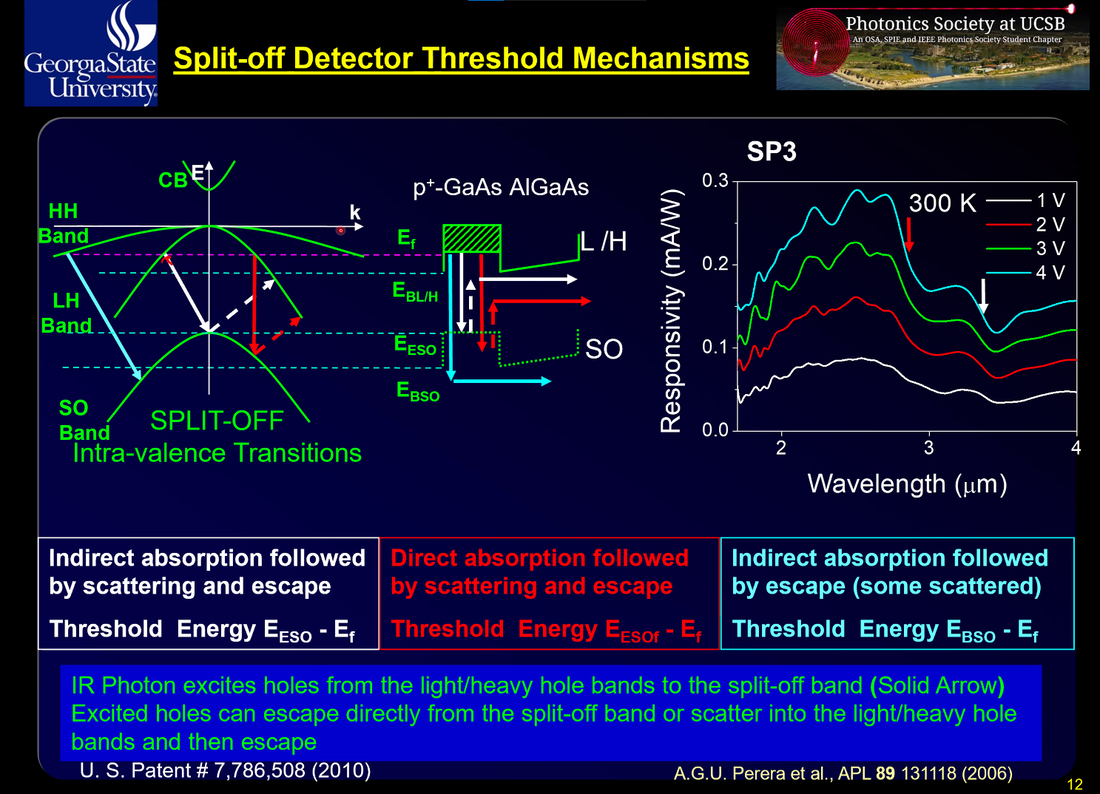
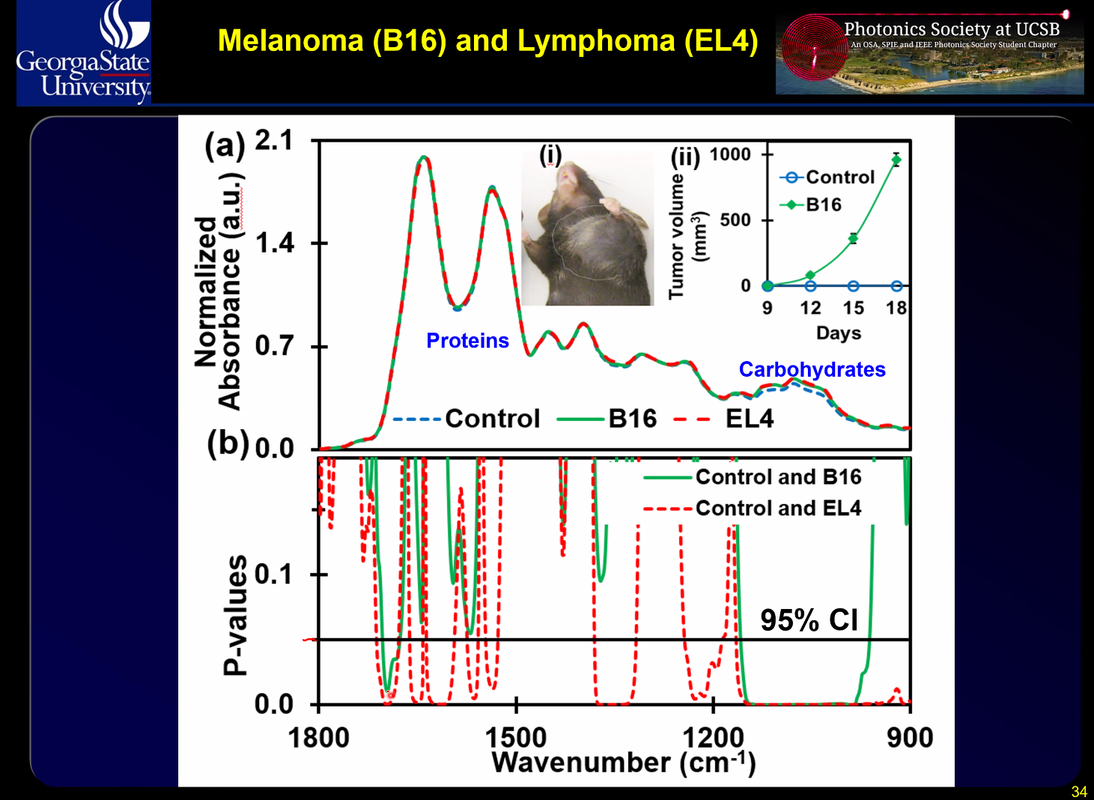
Friday, January 29th, 10 am (PST) Infrared detectors and imaging systems are becoming increasingly important in a diverse range of astronomic, military, and civilian applications. This field has gained significant attention while incorporating various materials and architectures into detector designs with a strong focus on applicability into clinical domains. Dr. Perera will discuss recent detector structures, and his latest work on disease detection. Biomedical applications of infrared include an exploration of an Affordable, Sensitive, Specific, User-friendly, Rapid, Equipment-free, and Deliverable (ASSURED) diagnostic regimen and testing its clinical feasibility for inflammatory bowel diseases (IBDs) and cancer screening. A study using Fourier transform infrared (FTIR) spectroscopy in attenuated total reflectance (ATR) sampling mode analyzed body fluids in order to identify reproducible, stable, and statistically significant differences in spectral signatures of the IR absorbance spectra between the control and disease samples. These results show that serum samples can be used to detect the biochemical changes induced by these diseases.
 1:00 PM Friday, January 22nd |
 Yahya Mohtashami Schuller group ECE Dept, UCSB |
In this talk, we show that we can increase the light extraction efficiency of, impart directionality upon, collimate, and focus the spontaneous emission from InGaN/GaN quantum wells, using phased-array metasurfaces. |
 |
Strong THz laser fields can explore non-linear, non-equilibrium phenomena in matter. The talk will focus on photons emitted by electron/hole re-collisions, and how the polarization of these photons carries information about the semiconductor. |
 | |
 |  |  |
 | On Henley Hall Prof. John Bowers |  |

 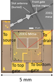 Schematic for the cross-section of a TACIT mixer (right); Optical image of a TACIT mixer with an SEM image of the active region (top) | Terahertz Heterodyne Detector Based on the Intersubband Transition of a GaAs/AlGaAs Quantum WellWe are developing a new type of THz heterodyne detector based on a high-mobility 2-dimensional electron gas (2DEG) in a GaAs/AlGaAs quantum well for spectroscopic applications in deep-space and planetary missions. Named as Tunable Antenna-Coupled Intersubband Terahertz (TACIT) mixer, the detector is a four-terminal hot-electron bolometer (HEB) mixer that uses intersubband transition for efficient absorption of THz radiation in a 2DEG. The dual gate structure of TACIT mixers, necessary for the precise control of the intersubband absorption characteristics, enables a high coupling efficiency at THz frequencies and tunability in the detection frequency, but also poses challenges in the fabrication, modelling, and operation of the device. In this talk, I will discuss our recent experimental results with a prototype TACIT mixer that we have fabricated with a flip-chip process that enables dual-side processing of a sub-micron thick quantum well membrane. 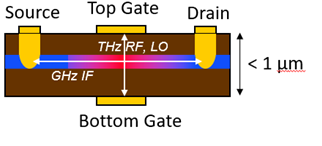 |
|
|

 Haojun Zhang DenBaars group ECE Dept, UCSB | Distributed feedback (DFB) laser diodes on GaNI will first talk about the recent work on blue III-Nitride LDs grown on semipolar GaN substrates. Then I will analyze the main hurdles that impeded its performance, focusing on improving the operating voltage, lifetime and mode quality, and discuss the efforts and approaches to further improve the efficiency and high-speed performance. |
 | Terahertz Heterodyne Detector Based on the Intersubband Transition of a GaAs/AlGaAs Quantum Well We are developing a new type of THz heterodyne detector based on a high-mobility 2DEG in a GaAs/AlGaAs quantum well for spectroscopic applications in deep-space and planetary missions. Named as Tunable Antenna-Coupled Intersubband Terahertz (TACIT) mixer, the detector uses intersubband transition for efficient absorption of THz radiation in a 2DEG. The dual gate structure of TACIT mixers, necessary for the precise control of the intersubband absorption characteristics, enables a high coupling efficiency at THz frequencies and tunability in the detection frequency, but also poses challenges in the fabrication, modelling, and operation of the device. In this talk, I will discuss our recent experimental results with a prototype TACIT mixer that we have fabricated with a flip-chip process that enables dual-side processing of a sub-micron thick quantum well membrane. |

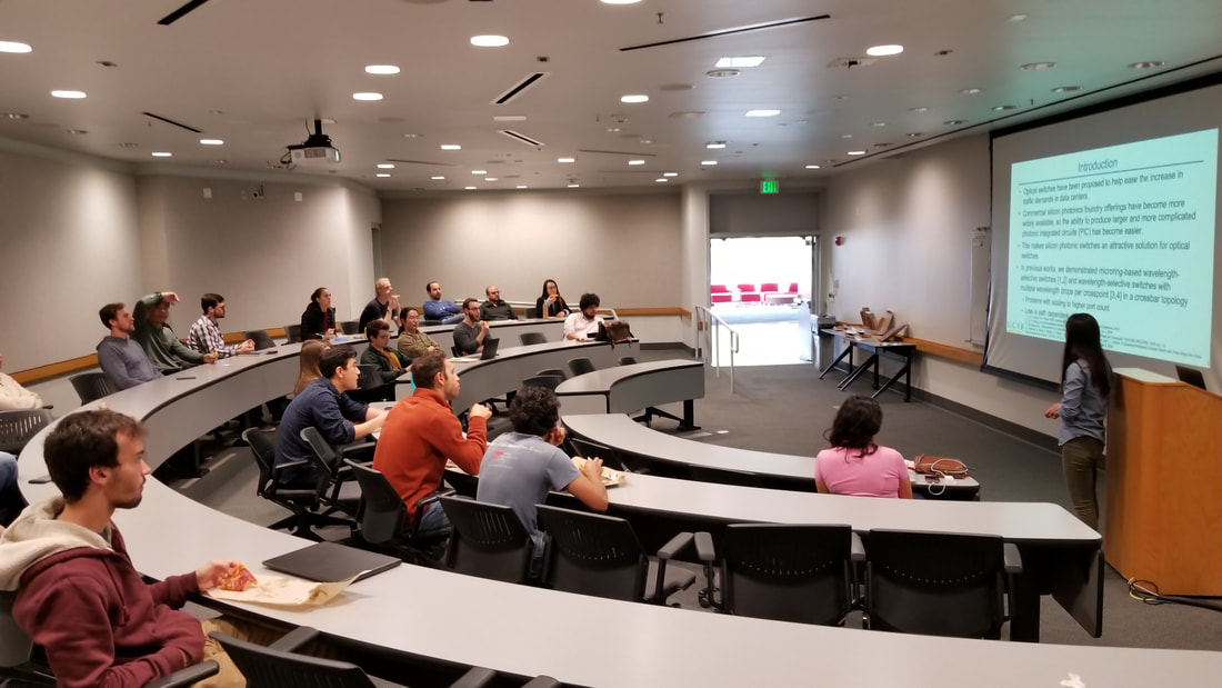
 | Ring-Assisted Mach-Zehnder Interferometer Switch with Multiple Rings per Switch ElementWavelength-selective switches have been propsed for datacenter use to help meet ever-increasing traffic demands. We present a 4-port silicon photonic ring-assisted Mach-Zehnder interferometer (RAMZI) switch, fabricated in the AIM Photonics process, with multiple-sized rings per switching element in a Benes network configuration to reduce the number of electrical pads required compared to a crossbar switch. Another advantage the RAMZI switch has over the crossbar switch is that the loss through the switch is not path-dependent due to its balanced path configuration. Finally, we present results from the fabricated switch co-packaged with a custom driver for control and discuss the outlook for further scaling of the switch architecture. |
 | Characterization of InGaN quatum dots grown by metal organic chemical vapor deposition (MOCVD)InGaN quantum dots were grown by metal organic chemical vapor deposition and shown to exhibit a bimodal size distribution. Atom probe tomography was used to characterize the dots in conjunction with atomic force microscopy (AFM), photoluminescence (PL), and x-ray diffraction (XRD). Small dots with low indium contents were found to coexist with larger, very high indium composition dots. The dots showed abrupt interfaces with the surrounding GaN, verifying the ability to cap the dots without causing intermixing for extremely high indium content dots. |
 | Advanced Semiconductor Lasers: Ultra-low Operating Energy and Hetergeneous Integration with Si Photonics Devices
|
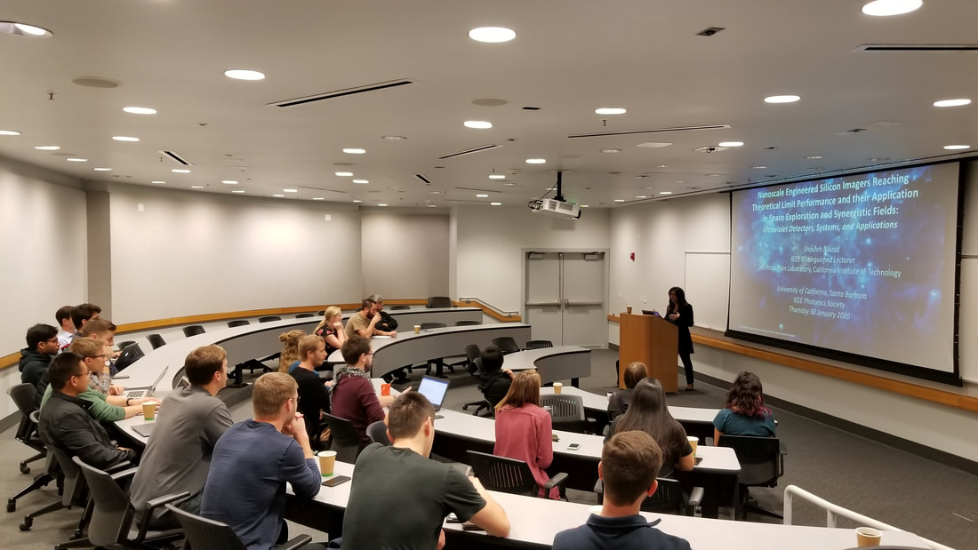
 | Nanoscale Engineered Silicon Imagers Reaching Theoretical Limit of Performance and their Applications in Space Exploration and Synergistic Fields Dr. Shouleh Nikzad NASA Jet Propulsion Laboratory |
 | Blue semipolar (20-2-1) vertical-cavity surface-emitting lasers with ion-implanted apertures and buried tunnel junction apertures (BTJ) are fabricated and compared to show that the BTJ's reduced absorption improves device performance. The effect of changing the out-coupling mirror reflectivity is calculated to project the potential of these devices with minor structural changes. |


May 2024
April 2024
March 2024
February 2024
January 2024
October 2023
August 2023
July 2023
June 2023
April 2023
March 2023
February 2023
January 2023
October 2022
September 2022
July 2022
June 2022
May 2022
April 2022
March 2022
February 2022
November 2021
October 2021
September 2021
July 2021
May 2021
April 2021
March 2021
January 2021
December 2020
October 2020
August 2020
May 2020
April 2020
February 2020
January 2020
December 2019
November 2019
October 2019
September 2019
July 2019
June 2019
May 2019
April 2019
February 2019
January 2019
December 2018
November 2018
October 2018
June 2018
February 2018
January 2018
October 2017
July 2017
June 2017
March 2017
February 2017
October 2016
September 2016
July 2016
April 2016
February 2016
January 2016
October 2015
September 2015
August 2015
July 2015
May 2015
January 2015
October 2014
September 2014
July 2014
May 2014
April 2014
March 2014
September 2013
July 2013
March 2013
February 2013
October 2012
All
Alumni Lectures
Industry Perspective Lectures
IPS Distinguished Lectures
Lectures
OSA Lectures
Outreach Events
Past Events
Social Events
Student Lecture Series